venerdì 21 dicembre 2012

From Umezawa to Vitiello: Quantum Field Theory of Brain States.

Source: Stanford Edu
-----------------------------
In the 1960s, Ricciardi and Umezawa (1967) suggested to utilize the formalism of quantum field theory to describe brain states, with particular emphasis on memory. The basic idea is to conceive of memory states in terms of states of many-particle systems, as inequivalent representations of vacuum states of quantum fields.[11] This proposal has gone through several refinements (e.g., Stuartet al. 1978, 1979; Jibu and Yasue 1995). Major recent progress has been achieved by including effects of dissipation, chaos, and quantum noise (Vitiello 1995; Pessa and Vitiello 2003). For readable nontechnical accounts of the approach in its present form, embedded in quantum field theory as of today, see Vitiello (2001, 2002).
Quantum field theory (see the entry on quantum field theory) yields infinitely many representations of the commutation relations, which are inequivalent to the Schrödinger representation of standard quantum mechanics. Such inequivalent representations can be generated by spontaneous symmetry breaking (see the entry on symmetry and symmetry breaking), occurring when the ground state (or the vacuum state) of a system is not invariant under the full group of transformations providing the conservation laws for the system. If symmetry breaks down, collective modes are generated (so-called Nambu-Goldstone boson modes), which propagate over the system and introduce long-range correlations in it.
These correlations are responsible for the emergence of ordered patterns. Unlike in thermal systems, a large number of bosons can be condensed in an ordered state in a highly stable fashion. Roughly speaking, this provides a quantum field theoretical derivation of ordered states in many-body systems described in terms of statistical physics. In the proposal by Umezawa these dynamically ordered states represent coherent activity in neuronal assemblies.
The activation of a neuronal assembly is necessary to make the encoded content consciously accessible. This activation is considered to be initiated by external stimuli. Unless the assembly is activated, its content remains unconscious, unaccessed memory. According to Umezawa, coherent neuronal assemblies correlated to such memory states are regarded as vacuum states; their activation leads to excited states with a finite lifetime and enables a conscious recollection of the content encoded in the vacuum (ground) state. The stability of such states and the role of external stimuli have been investigated in detail by Stuart et al. (1978, 1979).
A decisive further step in developing the approach has been achieved by taking dissipation into account. Dissipation is possible when the interaction of a system with its environment is considered. Vitiello (1995) describes how the system-environment interaction causes a doubling of the collective modes of the system in its environment. This yields infinitely many differently coded vacuum states, offering the possibility of many memory contents without overprinting. Moreover, dissipation leads to finite lifetimes of the vacuum states, thus representing temporally limited rather than unlimited memory (Alfinito and Vitiello 2000; Alfinito et al.2001). Finally, dissipation generates a genuine arrow of time for the system, and its interaction with the environment induces entanglement. In a recent contribution, Pessa and Vitiello (2003) have addressed additional effects of chaos and quantum noise.
The majority of presentations of this approach donot consistently distinguish between mental states and material states. This suggests reducibility of mental activity to brain activity, within scenario (A) of Sec. 2, as an underlying assumption. In this sense, Umezawa's proposal addresses the brain as a many-particle system as a whole, where the“particles” are more or less neurons. In the language of Section 3.1, this refers to the level of neuronal assemblies, which has the benefit that this is the level whichdirectly correlates with mental activity. Another merit of the quantum field theory approach is that it avoids the restrictions of standard quantum mechanics in a formally sound way.
Conceptually, however, it contains ambiguities demanding clarification, e.g., concerning the continuous confusion of mental and material states (and their properties). If mental states were the primary objects of reference, the quantum field theoretical treatment would be metaphorical in the sense of Section 4.1. That this is not the case has recently been clarified by Freeman and Vitiello (2008): the model “describes the brain, not mental states.”
For a description of brain states, it remains to be specified how this is backed up by the results of contemporary neurobiology. In recent publications (see, e.g., Freeman and Vitiello 2006, 2008), potential neurobiologically relevant observables such as electric and magnetic field amplitudes or neurotransmitter concentration have been discussed. These observables are purely classical, so that neurons, glia cells, “and other physiological units are not quantum objects in the many-body model of brain” (Freeman and Vitiello 2008).
This leads to the conclusion that the application of quantum field theory in the model serves the purpose of motivating that and why classical behavior emerges at the level of brain activity considered. The relevant brains states themselves are decidedly viewed as classical states. Similar to a classical thermodynamical description arising from quantum statistical mechanics, the idea is to identify different regimes of stable behavior (phases, attractors) and transitions between them. This way, quantum field theory provides formal elements from which a standard classical description of brain activity can be inferred, and this is its main role in the model.

martedì 16 ottobre 2012

Magnetic nanoparticles used to control thousands of cells simultaneously.

Source: Phys.org
--------------------------
Using clusters of tiny magnetic particles about 1,000 times smaller than the width of a human hair, researchers from the UCLA Henry Samueli School of Engineering and Applied Science have shown that they can manipulate how thousands of cells divide, morph and develop finger-like extensions.
This new tool could be used in developmental biology to understand how tissues develop, or in cancer research to uncover how cancer cells move and invade surrounding tissues, the researchers said. The UCLA team's findings were published online Oct. 14 in the journal Nature Methods. A cell can be considered a complex biological machine that receives an assortment of "inputs" and produces specific "outputs," such as growth, movement, division or the production of molecules. Beyond the type of input, cells are extremely sensitive to the location of an input, partly because cells perform "spatial multiplexing," reusing the same basic biochemical signals for different functions at different locations within the cell. Understanding this localization of signals is particularly challenging because scientists lack tools with sufficient resolution and control to function inside the miniature environment of a cell. And any usable tool would have to be able to perturb many cells with similar characteristics simultaneously to achieve an accurate distribution of responses, since the responses of individual cells can vary. To address this problem, an interdisciplinary UCLA team that included associate professor of bioengineering Dino Di Carlo, postdoctoral scholar Peter Tseng and professor of electrical engineering Jack Judy developed a platform to precisely manipulate magnetic nanoparticles inside uniformly shaped cells. These nanoparticles produced a local mechanical signal and yielded distinct responses from the cells.
By determining the responses of thousands of single cells with the same shape to local nanoparticle-induced stimuli, the researchers were able to perform an automated averaging of the cells' response. To achieve this platform, the team first had to overcome the challenge of moving such small particles (each measuring 100 nanometers) through the viscous interior of a cell once the cells engulfed them. Using ferromagnetic technologies, which enable magnetic materials to switch "on" and "off," the team developed an approach to embed a grid of small ferromagnetic blocks within a microfabricated glass slide and to precisely place individual cells in proximity to these blocks with a pattern of proteins that adhere to cells. When an external magnetic field is applied to this system, the ferromagnetic blocks are switched "on" and can therefore pull the nanoparticles within the cells in specific directions and uniformly align them. The researchers could then shape and control the forces in thousands of cells at the same time. Using this platform, the team showed that the cells responded to this local force in several ways, including in the way they divided. When cells go through the process of replication to create two cells, the axis of division depends on the shape of the cell and the anchoring points by which the cell holds on to the surface. The researchers found that the force induced by the nanoparticles could change the axis of cell division such that the cells instead divided along the direction of force. The researchers said this sensitivity to force may shed light on the intricate forming and stretching of tissues during embryonic development. Besides directing the axis of division, they found that nanoparticle-induced local force also led to the activation of a biological program in which cells generate filopodia, which are finger-like, actin-rich extensions that cells often use to find sites to adhere to and which aid in movement.
Di Carlo, the principal investigator on the research, envisions that the technique can apply beyond the control of mechanical stimuli in cells. "Nanoparticles can be coated with a variety of molecules that are important in cell signaling," he said. "We should now have a tool to quantitatively investigate how the precise location of molecules in a cell produces a specific behavior. This is a key missing piece in our tool-set for understanding cell programs and for engineering cells to perform useful functions." More information: www.nature.com/nmeth/journal/vaop/ncurrent/abs/nmeth.2210.html www.biomicrofluidics.com/ Provided by University of California, Los Angeles.

lunedì 15 ottobre 2012

Graphene researchers make a layer cake with atomic precision.

Source: Phys.org
--------------------------
Graphene and associated one-atom-thick crystals offer the possibility of a vast range of new materials and devices by stacking individual atomic layers on top of each other, new research from the University of Manchester shows.
In a report published in Nature Physics, a group led Dr Leonid Ponomarenko and Nobel prize-winner Professor Andre Geim has assembled individual atomic layers on top of each other in a desired sequence. The team used individual one-atom-thick crystals to construct a multilayer cake that works as a nanoscale electric transformer. Graphene, isolated for the first time at The University of Manchester in 2004, has the potential to revolutionise diverse applications from smartphones and ultrafast broadband to drug delivery and computer chips. It has the potential to replace existing materials, such as silicon, but the Manchester researchers believe it could truly find its place with new devices and materials yet to be invented. In the nanoscale transformer, electrons moving in one metallic layer pull electrons in the second metallic layer by using their local electric fields. To operate on this principle, the metallic layers need to be insulated electrically from each other but separated by no more than a few interatomic distances, a giant leap from the existing nanotechnologies. These new structures could pave the way for a new range of complex and detailed electronic and photonic devices which no other existing material could make, which include various novel architectures for transistors and detectors. The scientists used graphene as a one-atom-thick conductive plane while just four atomic layers of boron nitride served as an electrical insulator.
The researchers started with extracting individual atomic planes from bulk graphite and boron nitride by using the same technique that led to the Nobel Prize for graphene, a single atomic layer of carbon. Then, they used advanced nanotechnology to mechanically assemble the crystallites one by one, in a Lego style, into a crystal with the desired sequence of planes. The nano-transformer was assembled by Dr Roman Gorbachev, of The University of Manchester, who described the required skills. He said: "Every Russian and many in the West know The Tale of the Clockwork Steel Flea. "It could only be seen through the most powerful microscope but still danced and even had tiny horseshoes. Our atomic-scale Lego perhaps is the next step of craftsmanship". Professor Geim added: "The work proves that complex devices with various functionalities can be constructed plane by plane with atomic precision. "There is a whole library of atomically-thin materials. By combining them, it is possible to create principally new materials that don't exist in nature. This avenue promises to become even more exciting than graphene itself." More information: 'Strong Coulomb drag and broken symmetry in double-layer graphene', by L Ponomarenko, R Gorbachev and A Geim, Nature Physics, 2012.Journal reference: Nature Physics Provided by University of Manchester.

Accelerators can search for signs of Planck-scale gravity.

Source: Phys.org
--------------------------
Although quantum theory can explain three of the four forces in nature, scientists currently rely on general relativity to explain the fourth force, gravity. However, no one is quite sure of how gravity works at very short distances, in particular the shortest distance of all: the Planck length, or 10^-35 m. So far, the smallest distance accessible in experiments is about 10^-19 m at the LHC.
Now in a new paper published in Physical Review Letters, physicist Vahagn Gharibyan of Deutsches Elektronen-Synchrotron (DESY) in Hamburg, Germany, has proposed a test of quantum gravity that can reach a sensitivity of 10^-31 m down to the Planck length, depending on the energy of the particle accelerator. As Gharibyan explains, several models of quantum gravity predict that empty space near the Planck length may behave like a crystal in the sense that the space is refractive (light is bent due to "gravitons," the hypothetical particles that mediate gravity) and has birefringence/chirality (the light's bending degree also depends on the light's polarization). In quantum gravity, both refractivity and birefringence are energy-dependent: the higher the photon energy, the stronger the photon-graviton interaction and the more bending. This correlation is the opposite of what happens when photons interact with electromagnetic fields or matter, where these effects are suppressed by photon energy. The predicted correlation also differs from what happens according to Newtonian gravity and Einstein's general relativity, where any bending of light is independent of the light's energy. "If one describes gravity at the quantum level, the bending of light by gravitation becomes energy-dependent – unlike in Newtonian gravity or Einstein's general relativity," Gharibyan told Phys.org. "The higher the energy of the photons, the larger the bending, or the stronger the photon-graviton interaction should be."
Gharibyan suggests that this bending of light according to quantum gravity models may be studied using high-energy accelerator beams that probe the vacuum symmetry of empty space at small scales. Accelerators could use high-energy Compton scattering, in which a photon that scatters off another moving particle acquires energy, causing a change in its momentum. The proposed experiments could detect how the effects of quantum gravity change the photon's energy-momentum relation compared with what would be expected on a normal scale. For these experiments, the beam energy is vital in determining the sensitivity to small-scale effects. Gharibyan estimates that a 6 GeV energy lepton accelerator, such as PETRA-III at DESY, could test space birefringence down to 10^-31 m. Future accelerators that could achieve energies of up to 250 GeV, such as the proposed International Linear Collider (ILC), could test birefringence all the way down to the Planck length. For probing refractivity, Gharibyan estimates that a 6 GeV machine would have a sensitivity down to 10^-27 m, while a 250 GeV machine could reach about 10^-31 m. As Gharibyan explains, probing Planck-scale gravity in this way is somewhat similar to investigating nanoscale crystal structures.
"Conventional crystals have cell sizes around tens of nanometers and are transparent to, or do not interact with, photons with much larger (m or mm) wavelengths," Gharibyan said. "In order to investigate crystal cells/structures, one needs photons with compatible nm wavelength: X-rays. However, visible light with wavelengths 1000 times more than the crystal cell can still feel the averaged influence of the cells: the light could be reflected singly or doubly. Comparing this to the Planck-length crystal, we don't have photons with a Planck wavelength or that huge energy. Instead, we are able to feel the averaged effects of Planck crystal cells – or space grains – by using much [relatively] lower-energy photons." In fact, as Gharibyan has found, there are already experimental hints of gravitons. "This work presents evidence for quantum gravity interactions by applying the developed method to gamma rays faster than light, which I found earlier in data from the largest US and German electron accelerators," he said. "The absence of any starlight deflection in the cosmic vacuum hints that Earth's gravitons should be considered responsible for the observed bending of the accelerators' gamma rays." Gharibyan found that data from the now-closed 26.5 GeV Hadron-Electron Ring Accelerator (HERA) at DESY measured a Planck cell size of 2.6x10^-28 m, and data from the mothballed 45.6 GeV Stanford Linear Collider (SLC) at Stanford University in the US measured a space grain size of 3.5x10^-30 m. While these results provide some hints of Planck-scale gravity, neither of these experiments was designed as a tool to specifically test gravity, so Gharibyan warns that uncontrolled pieces of setups could mimic observed effects.
If Gharibyan's newly proposed experiments are performed, they would provide the first direct measurements of space near or even at the Planck scale, and by doing so, offer a closer glimpse of gravity in this enigmatic regime. More information: Vahagn Gharibyan. "Testing Planck-Scale Gravity with Accelerators." Physical Review Letters 109, 141103 (2012). DOI: 10.1103/PhysRevLett.109.141103 Vahagn Gharibyan. "Possible observation of photon speed energy dependence." Physics Letters B 611 231-238 (2005). DOI: 10.1016/j.physletb.2005.02.053

Quantum oscillator responds to pressure.

Source: Phys.org
----------------------
In the far future, superconducting quantum bits might serve as components of high-performance computers. Today already do they help better understand the structure of solids, as is reported by researchers of Karlsruhe Institute of Technology in the Science magazine. By means of Josephson junctions, they measured the oscillations of individual atoms "tunneling" be-tween two positions. This means that the atoms oscillated quantum mechanically. Deformation of the specimen even changed the frequency. 
"We are now able to directly control the frequencies of individual tunneling atoms in the solid," say Alexey Ustinov and Georg Weiß, Professors at the Physikalisches Institut of KIT and members of the Center for Functional Nanostructures CFN. Metaphorically speaking, the researchers so far have been confronted with a closed box. From inside, different clattering noises could be heard. Now, it is not only possible to measure the individual objects contained, but also to change their physical properties in a controlled manner. The specimen used for this purpose consists of a superconducting ring interrupted by a nanometer-thick non-conductor, a so-called Josephson junction. The qubit formed in this way can be switched very precisely between two quantum states. "Interestingly, such a Josephson qubit couples to the other atomic quantum systems in the non-conductor," explains Ustinov. "And we measure their tunneling frequencies via this coupling." At temperatures slightly above absolute zero, most sources of noise in the material are switched off. The only remaining noise is produced by atoms of the material when they jump between two equivalent positions. "These frequency spectra of atom jumps can be measured very precisely with the Josephson junction," says Ustinov. "Metaphorically speaking, we have a microscope for the quantum mechanics of individual atoms." In the experiment performed, 41 jumping atoms were counted and their frequency spectra were measured while the specimen was bent slightly with a piezo element. Georg Weiß explains: "The atomic dis-tances are changed slightly only, while the frequencies of the tunneling atoms change strongly." So far, only the sum of all tunneling atoms could be measured. The technology to separately switch atomic tunneling systems only emerged a few years ago. The new method developed at KIT to control atomic quantum systems might provide valuable insights into how qubits can be made fit for applica-tion. However, the method is also suited for studying materials of conventional electronic components, such as transistors, and estab-lishing the basis of further miniaturization. More information: DOI: 10.1126/science.1226487 Provided by Karlsruhe Institute of Technology.

sabato 13 ottobre 2012

Physicists propose method to determine if the universe is a simulation.

Source: Phys.org
-------------------------
(Phys.org)—A common theme of science fiction movies and books is the idea that we're all living in a simulated universe—that nothing is actually real. This is no trivial pursuit: some of the greatest minds in history, from Plato, to Descartes, have pondered the possibility. Though, none were able to offer proof that such an idea is even possible. Now, a team of physicists working at the University of Bonn have come up with a possible means for providing us with the evidence we are looking for; namely, a measurable way to show that our universe is indeed simulated. They have written a paper describing their idea and have uploaded it to the preprint server arXiv.
The team's idea is based on work being done by other scientists who are actively engaged in trying to create simulations of our universe, at least as we understand it. Thus far, such work has shown that to create a simulation of reality, there has to be a three dimensional framework to represent real world objects and processes. With computerized simulations, it's necessary to create a lattice to account for the distances between virtual objects and to simulate the progression of time. The German team suggests such a lattice could be created based on quantum chromodynamics—theories that describe the nuclear forces that bind subatomic particles. To find evidence that we exist in a simulated world would mean discovering the existence of an underlying lattice construct by finding its end points or edges. In a simulated universe a lattice would, by its nature, impose a limit on the amount of energy that could be represented by energy particles. This means that if our universe is indeed simulated, there ought to be a means of finding that limit. In the observable universe there is a way to measure the energy of quantum particles and to calculate their cutoff point as energy is dispersed due to interactions with microwaves and it could be calculated using current technology. Calculating the cutoff, the researchers suggest, could give credence to the idea that the universe is actually a simulation. Of course, any conclusions resulting from such work would be limited by the possibility that everything we think we understand about quantum chromodynamics, or simulations for that matter, could be flawed.
 
More information: Constraints on the Universe as a Numerical Simulation, arXiv:1210.1847 [hep-ph] arxiv.org/abs/1210.1847  
 
Abstract:
Observable consequences of the hypothesis that the observed universe is a numerical simulation performed on a cubic space-time lattice or grid are explored. The simulation scenario is first motivated by extrapolating current trends in computational resource requirements for lattice QCD into the future. Using the historical development of lattice gauge theory technology as a guide, we assume that our universe is an early numerical simulation with unimproved Wilson fermion discretization and investigate potentially-observable consequences. Among the observables that are considered are the muon g-2 and the current differences between determinations of alpha, but the most stringent bound on the inverse lattice spacing of the universe, b^(-1) >~ 10^(11) GeV, is derived from the high-energy cut off of the cosmic ray spectrum. The numerical simulation scenario could reveal itself in the distributions of the highest energy cosmic rays exhibiting a degree of rotational symmetry breaking that reflects the structure of the underlying lattice.
Journal reference: arXiv

giovedì 11 ottobre 2012

Nanoparticles: Making Gold Economical for Sensing.

Source: ScienceDaily
-------------------------------
ScienceDaily (Oct. 10, 2012) — Gold nanocluster arrays developed at A*STAR are well suited for commercial applications of a high-performance sensing technique.
Cancer, food pathogens and biosecurity threats can all be detected using a sensing technique called surface enhanced Raman spectroscopy (SERS). To meet ever-increasing demands in sensitivity, however, signals from molecules of these agents require massive enhancement, and current SERS sensors require optimization. An A*STAR-led research team recently fabricated a remarkably regular array of closely packed gold nanoparticle clusters that will improve SERS sensors.
So-called 'Raman scattering' occurs when molecules scatter at wavelengths not present in the incident light. These molecules can be detected with SERS sensors by bringing them into contact with a nanostructured metal surface, illuminated by a laser at a particular wavelength. An ideal sensor surface should have: dense packing of metal nanostructures, commonly gold or silver, to intensify Raman scattering; a regular arrangement to produce repeatable signal levels; economical construction; and robustness to sustain sensing performance over time.
Few of the many existing approaches succeed in all categories. However, Fung Ling Yap and Sivashankar Krishnamoorthy at the A*STAR Institute of Materials Research and Engineering, Singapore, and co-workers produced closely packed nanocluster arrays of gold that incorporate the most desirable aspects for fabrication and sensing. In addition to flat surfaces, they also succeeded in coating fiber-optic tips with similarly dense nanocluster arrays (see image), which is a particularly promising development for remote-sensing applications, such as hazardous waste monitoring.
The researchers self-assembled their arrays by using surfaces coated with self-formed polymer nanoparticles, to which smaller gold nanoparticles spontaneously attached to form clusters. "It was surprising to reliably attain feature separations of less than 10 nanometers, at high yield, across macroscopic areas using simple processes such as coating and adsorption," notes Krishnamoorthy.
By varying the size and density of the polymer features, Krishnamoorthy, Yap and co-workers tuned the cluster size and density to maximize SERS enhancements. Their technique is also efficient: less than 10 milligrams of the polymer and 100 milligrams of gold nanoparticles are needed to coat an entire 100 millimeter diameter wafer, or approximately 200 fiber tips. Both the polymer and the nanoparticles can be mass-produced at low cost. By virtue of being entirely 'self-assembled', the technique does not require specialized equipment or a custom-built clean room, so it is well suited to low-cost commercial implementation.
"We have filed patent applications for the work in Singapore, the USA and China," says Krishnamoorthy. "The arrays are close to commercial exploitation as disposable sensor chips for use in portable SERS sensors, in collaboration with industry."

sabato 29 settembre 2012

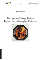
"The synchro energy project, beyond the holographic universe"; e-book, pp.188, 5 USD.

--------------------------------------


This volume includes, for the first time, a description of the first experimental results of the Synchro Energy Project; it is a project created approximately two years ago, which brings forward the merging of concepts of Synchronicity (Jungian), Non-locality and wave function collapse. The experiments were carried out in a small research laboratory in Switzerland (near the University of Lausanne) with the collaboration of: Patrick Reiner (Theoric Physicist,PhD), Jean-Michel Bonnet (electronic engineer,PhD) and Christine Duval (neuropsychologist and physiologist). This volume therefore exposes and explains for the first time, the theoretical and experimental basis sustaining the "Principle of Quantum Compensation of Subconscious Nucleuses". It will therefore provide a careful reader some excellent points for reflexion in relation to an ambit that has still been completely unexplored within the field of research of interaction between psyche and matter.
.
Fausto Intilla, inventor and scientific popularizer, is of Italian origin but lives and works in Switzerland (Ticino County). In the editing sector, he made his debut in 1995 with “Journey beyond this life” (ed. Nuovi Autori, Milano), a captivating science fiction story which witnesses the polyhedral nature of the author. His last books are: "Dio=mc2. Oltre l'Universo Olografico" and "La funzione d'onda della Realtà" . English books by Fausto Intilla: "The Synchro Energy Project, beyond the Holographic Universe". In the field of inventions, however, his name is linked to the “Tree Structure” , one of the most popular anti-seismic structures for bridges and viaducts patented in Japan and in the United States (see: www.uspto.gov) . His e-mail address is: f.intilla@bluewin.ch

Intilla, is also the creator of “Principle of Quantum Compensation of Subconscious Nucleuses”. His research on subconscious nucleuses and the experiments proposed by him for the verification of such Principle, have been taken into consideration by several research groups in both Europe and the United States;one of these is the renowned P.E.A.R. laboratory (Princeton Engineering Anomalies Research) situated in New Jersey, USA. The research in this science by Dr.Roger D.Nelson and colleagues, after the recent closure of the PEAR laboratory, were transferred here: ICRL. In this Institute, for several years, the research has been directed mainly toward the "Global Consciousness Project".

martedì 28 febbraio 2012

Quantum Microphone Captures Extremely Weak Sound.

A "quantum microphone" based on a Single Electron Transistor (SET) detects sound waves on a chip surface, so called Surface Acoustic Waves (SAW). The waves make the charge of the atoms underneath the quantum microphon oscillate. Since the quantum microphone is an extremely sensitive charge detector, very low sound levels can be detected. (The size of the waves are exaggerated in the picture). (Credit: Philip Krantz, Chalmers)
Source: Science Daily
-------------------------------------
ScienceDaily (Feb. 27, 2012) — Scientists from Chalmers University of Technology have demonstrated a new kind of detector for sound at the level of quietness of quantum mechanics. The result offers prospects of a new class of quantum hybrid circuits that mix acoustic elements with electrical ones, and may help illuminate new phenomena of quantum physics.
The results have been published in Nature Physics.
The "quantum microphone" is based on a single electron transistor, that is, a transistor where the current passes one electron at a time. The acoustic waves studied by the research team propagate over the surface of a crystalline microchip, and resemble the ripples formed on a pond when a pebble is thrown into it. The wavelength of the sound is a mere 3 micrometers, but the detector is even smaller, and capable of rapidly sensing the acoustic waves as they pass by.
On the chip surface, the researchers have fabricated a three-millimeter-long echo chamber, and even though the speed of sound on the crystal is ten times higher than in air, the detector shows how sound pulses reflect back and forth between the walls of the chamber, thereby verifying the acoustic nature of the wave.
The detector is sensitive to waves with peak heights of a few percent of a proton diameter, levels so quiet that sound can be governed by quantum law rather than classical mechanics, much in the same way as light.
"The experiment is done on classical acoustic waves, but it shows that we have everything in place to begin studies of proper quantum-acoustics, and nobody has attempted that before," says Martin Gustafsson, PhD student and first author of the article.
Apart from the extreme quietness, the pitch of the waves is too high for us to hear: The frequency of almost 1 gigahertz is 21 octaves above one-lined A. The new detector is the most sensitive in the world for such high-frequency sound.

lunedì 27 febbraio 2012

Replacing Electricity With Light: First Physical 'Metatronic' Circuit Created.

Figure A. When the plane of the electric field is in line with the nanorods the circuit is wired in parallel. Figure B. When the plane of the electric field crosses both the nanorods and the gaps the circuit is wired in series. (Credit: Image courtesy of University of Pennsylvania).
Source: Science Daily
----------------------------------
ScienceDaily (Feb. 23, 2012) — The technological world of the 21st century owes a tremendous amount to advances in electrical engineering, specifically, the ability to finely control the flow of electrical charges using increasingly small and complicated circuits. And while those electrical advances continue to race ahead, researchers at the University of Pennsylvania are pushing circuitry forward in a different way, by replacing electricity with light.

"Looking at the success of electronics over the last century, I have always wondered why we should be limited to electric current in making circuits," said Nader Engheta, professor in the electrical and systems engineering department of Penn's School of Engineering and Applied Science. "If we moved to shorter wavelengths in the electromagnetic spectrum -- like light -- we could make things smaller, faster and more efficient."
Different arrangements and combinations of electronic circuits have different functions, ranging from simple light switches to complex supercomputers. These circuits are in turn built of different arrangements of circuit elements, like resistors, inductors and capacitors, which manipulate the flow of electrons in a circuit in mathematically precise ways. And because both electric circuits and optics follow Maxwell's equations -- the fundamental formulas that describe the behavior of electromagnetic fields -- Engheta's dream of building circuits with light wasn't just the stuff of imagination. In 2005, he and his students published a theoretical paper outlining how optical circuit elements could work.
Now, he and his group at Penn have made this dream a reality, creating the first physical demonstration of "lumped" optical circuit elements. This represents a milestone in a nascent field of science and engineering Engheta has dubbed "metatronics."
Engheta's research, which was conducted with members of his group in the electrical and systems engineering department, Yong Sun, Brian Edwards and Andrea Alù, was published in the journal Nature Materials.
In electronics, the "lumped" designation refers to elements that can be treated as a black box, something that turns a given input to a perfectly predictable output without an engineer having to worry about what exactly is going on inside the element every time he or she is designing a circuit.
"Optics has always had its own analogs of elements, things like lenses, waveguides and gratings," Engheta said, "but they were never lumped. Those elements are all much larger than the wavelength of light because that's all that could be easily built in the old days. For electronics, the lumped circuit elements were always much smaller than the wavelength of operation, which is in the radio or microwave frequency range."
Nanotechnology has now opened that possibility for lumped optical circuit elements, allowing construction of structures that have dimensions measured in nanometers. In this experiment's case, the structure was comb-like arrays of rectangular nanorods made of silicon nitrite.
The "meta" in "metatronics" refers to metamaterials, the relatively new field of research where nanoscale patterns and structures embedded in materials allow them to manipulate waves in ways that were previously impossible. Here, the cross-sections of the nanorods and the gaps between them form a pattern that replicates the function of resistors, inductors and capacitors, three of the most basic circuit elements, but in optical wavelengths.
"If we have the optical version of those lumped elements in our repertoire, we can actually make designs similar to what we do in electronics but now for operation with light," Engheta said. "We can build a circuit with light."
In their experiment, the researchers illuminated the nanorods with an optical signal, a wave of light in the mid-infrared range. They then used spectroscopy to measure the wave as it passed through the comb. Repeating the experiment using nanorods with nine different combinations of widths and heights, the researchers showed that the optical "current" and optical "voltage" were altered by the optical resistors, inductors and capacitors with parameters corresponding to those differences in size.
"A section of the nanorod acts as both an inductor and resistor, and the air gap acts as a capacitor," Engheta said.
Beyond changing the dimensions and the material the nanorods are made of, the function of these optical circuits can be altered by changing the orientation of the light, giving metatronic circuits access to configurations that would be impossible in traditional electronics.
This is because a light wave has polarizations; the electric field that oscillates in the wave has a definable orientation in space. In metatronics, it is that electric field that interacts and is changed by elements, so changing the field's orientation can be like rewiring an electric circuit.
When the plane of the field is in line with the nanorods, as in Figure A, the circuit is wired in parallel and the current passes through the elements simultaneously. When the plane of the electric field crosses both the nanorods and the gaps, as in Figure B, the circuit is wired in series and the current passes through the elements sequentially.
"The orientation gives us two different circuits, which is why we call this 'stereo-circuitry,'" Engheta said. "We could even have the wave hit the rods obliquely and get something we don't have in regular electronics: a circuit that's neither in series or in parallel but a mixture of the two."
This principle could be taken to an even higher level of complexity by building nanorod arrays in three dimensions. An optical signal hitting such a structure's top would encounter a different circuit than a signal hitting its side. Building off their success with basic optical elements, Engheta and his group are laying the foundation for this kind of complex metatronics.
"Another reason for success in electronics has to do with its modularity," he said. "We can make an infinite number of circuits depending on how we arrange different circuit elements, just like we can arrange the alphabet into different words, sentences and paragraphs.
"We're now working on designs for more complicated optical elements," Engheta said. "We're on a quest to build these new letters one by one."
This work was supported in part by the U.S. Air Force Office of Scientific Research.
Andrea Alù is now an assistant professor at the University of Texas at Austin.

Scientists Score New Victory Over Quantum Uncertainty.

Michael Chapman, a professor in the School of Physics at Georgia Tech, poses with optical equipment in his laboratory. Chapman’s research team is exploring squeezed states using atoms of Bose-Einstein condensates. (Click image for high-resolution version. Credit: Gary Meek) (Credit: Image courtesy of Georgia Institute of Technology, Research Communications)
Source: Science Daily
-------------------------------
ScienceDaily (Feb. 26, 2012) — Most people attempt to reduce the little uncertainties of life by carrying umbrellas on cloudy days, purchasing automobile insurance or hiring inspectors to evaluate homes they might consider purchasing. For scientists, reducing uncertainty is a no less important goal, though in the weird realm of quantum physics, the term has a more specific meaning.
For scientists working in quantum physics, the Heisenberg Uncertainty Principle says that measurements of properties such as the momentum of an object and its exact position cannot be simultaneously specified with arbitrary accuracy. As a result, there must be some uncertainty in either the exact position of the object, or its exact momentum. The amount of uncertainty can be determined, and is often represented graphically by a circle showing the area within which the measurement actually lies.
Over the past few decades, scientists have learned to cheat a bit on the Uncertainty Principle through a process called "squeezing," which has the effect of changing how the uncertainty is shown graphically. Changing the circle to an ellipse and ultimately to almost a line allows one component of the complementary measurements -- the momentum or the position, in the case of an object -- to be specified more precisely than would otherwise be possible. The actual area of uncertainty remains unchanged, but is represented by a different shape that serves to improve accuracy in measuring one property.
This squeezing has been done in measuring properties of photons and atoms, and can be important to certain high-precision measurements needed by atomic clocks and the magnetometers used to create magnetic resonance imaging views of structures deep inside the body. For the military, squeezing more accuracy could improve the detection of enemy submarines attempting to hide underwater or improve the accuracy of atom-based inertial guidance instruments.
Now physicists at the Georgia Institute of Technology have added another measurement to the list of those that can be squeezed. In a paper appearing online February 26 in the journal Nature Physics, they report squeezing a property called the nematic tensor, which is used to describe the rubidium atoms in Bose-Einstein condensates, a unique form of matter in which all atoms have the same quantum state. The research was sponsored by the National Science Foundation (NSF).
"What is new about our work is that we have probably achieved the highest level of atom squeezing reported so far, and the more squeezing you get, the better," said Michael Chapman, a professor in Georgia Tech's School of Physics. "We are also squeezing something other than what people have squeezed before."
Scientists have been squeezing the spin states of atoms for 15 years, but only for atoms that have just two relevant quantum states -- known as spin ½ systems. In collections of those atoms, the spin states of the individual atoms can be added together to get a collective angular momentum that describes the entire system of atoms.
In the Bose-Einstein condensate atoms being studied by Chapman's group, the atoms have three quantum states, and their collective spin totals zero -- not very helpful for describing systems. So Chapman and graduate students Chris Hamley, Corey Gerving, Thai Hoang and Eva Bookjans learned to squeeze a more complex measure that describes their system of spin 1 atoms: nematic tensor, also known as quadrupole.
Nematicity is a measure of alignment that is important in describing liquid crystals, exotic magnetic materials and some high temperature superconductors.
"We don't have a spin vector pointing in a particular direction, but there is still some residual information in where this collection of atoms is pointing," Chapman explained. "That next higher-order description is the quadrupole, or nematic tensor. Squeezing this actually works quite well, and we get a large degree of improvement, so we think it is relatively promising."
Experimentally, the squeezing is created by entangling some of the atoms, which takes away their independence. Chapman's group accomplishes this by colliding atoms in their ensemble of some 40,000 rubidium atoms.
"After they collide, the state of one atom is connected to that of the other atom, so they have been entangled in that way," he said. "This entanglement creates the squeezing."
Reducing uncertainty in measuring atoms could have important implications for precise magnetic measurements. The next step will be to determine experimentally if the technique can improve the measurement of magnetic field, which could have important applications.
"In principle, this should be a straightforward experiment, but it turns out that the biggest challenge is that magnetic fields in the laboratory fluctuate due to environmental factors such as the effects of devices such as computer monitors," Chapman said. "If we had a noiseless laboratory, we could measure the magnetic field both with and without squeezed states to demonstrate the enhanced precision. But in our current lab environment, our measurements would be affected by outside noise, not the limitations of the atomic sensors we are using."
The new squeezed property could also have application to quantum information systems, which can store information in the spin of atoms and their nematic tensor.
"There are a lot of things you can do with quantum entanglement, and improving the accuracy of measurements is one of them," Chapman added. "We still have to obey Heisenberg's Uncertainty Principle, but we do have the ability to manipulate it."