mercoledì 31 ottobre 2007

Silicon Can Work For New-Age Spintronics Applications


Source:

ScienceDaily (Oct. 31, 2007) — In a rapid follow-up to their achievement as the first to demonstrate how an electron's spin can be electrically injected, controlled and detected in silicon, electrical engineers from the University of Delaware and Cambridge NanoTech now show that this quantum property can be transported a marathon distance in the world of microelectronics-- through an entire silicon wafer.
The finding confirms that silicon--the workhorse material of present-day electronics--now can be harnessed up for new-age spintronics applications.
The results mark another major steppingstone in the pioneering field of spintronics, which aims to use the intrinsic “spin” property of electrons versus solely their electrical charge for the cheaper, faster, lower-power processing and storage of data than present-day electronics can offer.
The research team included Ian Appelbaum, UD assistant professor of electrical and computer engineering, and his doctoral student, Biqin Huang, and Douwe Monsma, of Cambridge NanoTech in Cambridge, Mass. Huang was the lead author of the article.*
“Our new result is significant because it means that silicon can now be used to perform many spin manipulations both within the space of thousands of devices and within the time of thousands of logic operations, paving the way for silicon-based spintronics circuits,” Appelbaum said.
In Appelbaum's lab at UD, the team fabricated a device that injected high-energy, “hot” electrons from a ferromagnet into the silicon wafer. Another hot-electron structure (made by bonding two silicon wafers together with a thin-film ferromagnet) detected the electrons on the other side.
“Electron spin has a direction, like 'up' or 'down,' ” Appelbaum said. “In silicon, there are normally equal numbers of spin-up and -down electrons. The goal of spintronics is to use currents with most of the electron spins oriented, or polarized, in the same direction.”
In another recent paper published in the Aug. 13 issue of Applied Physics Letters, the team showed how to attain very high spin polarization, achieving more than 37 percent, and then demonstrated operation as the first semiconductor spin field-effect transistor.
“One hundred percent polarization means that all injected electrons are either spin-up or spin-down,” Huang explained. “High polarization will be necessary for practical applications.”
“In the future, spintronics may bring a great change to daily life,” Huang added.
“We're taking the first steps at the beginning of a new road,” Appelbaum said. “Before our initial work on spin transport in silicon, we didn't even know where the road was,” he said with a smile. “There's a lot of fundamental work to be done, which we hope will bring us closer to a new age of electronics.”
*The article was published in the Oct. 26 issue of the American Physical Society's journal Physical Review Letters.
Adapted from materials provided by University of Delaware.

Fausto Intilla

Star Trek Gadget? 'Tractor Beam' For Cells Developed


Source:

ScienceDaily (Oct. 31, 2007) — In a feat that seems like something out of a microscopic version of Star Trek, MIT researchers have found a way to use a “tractor beam” of light to pick up, hold, and move around individual cells and other objects on the surface of a microchip.
The new technology could become an important tool for both biological research and materials research, say Matthew J. Lang and David C. Appleyard, whose work is being published in the journal Lab on a Chip.
The idea of using light beams as tweezers to manipulate cells and tiny objects has been around for at least 30 years. But the MIT researchers have found a way to combine this powerful tool for moving, controlling and measuring objects with the highly versatile world of microchip design and manufacturing.
Optical tweezers, as the technology is known, represent “one of the world's smallest microtools,” says Lang. “Now, we're applying it to building [things] on a chip.”
Says Appleyard, “We've shown that you could merge everything people are doing with optical trapping with all the exciting things you can do on a silicon wafer…There could be lots of uses at the biology-and-electronics interface.”
For example, he said, many people are studying how neurons communicate by depositing them on microchips where electrical circuits etched into the chips monitor their electrical behavior. “They randomly put cells down on a surface, and hope one lands on [or near] a [sensor] so its activity can be measured. With [our technology], you can put the cell right down next to the sensors.” Not only can motions be precisely controlled with the device, but it can also provide very precise measurements of a cell's position.
Optical tweezers use the tiny force of a beam of light from a laser to push around and control tiny objects, from cells to plastic beads. They usually work on a glass surface mounted inside a microscope so that the effects can be observed.
But silicon chips are opaque to light, so applying this technique to them not an obvious move, the researchers say, since the optical tweezers use light beams that have to travel through the material to reach the working surface. The key to making it work in a chip is that silicon is transparent to infrared wavelengths of light - which can be easily produced by lasers, and used instead of the visible light beams.
To develop the system, Lang and Appleyard weren't sure what thickness and surface texture of wafers, the thin silicon slices used to manufacture microchips, would work best, and the devices are expensive and usually available only in quantity. “Being at MIT, where there is such a strength in microfabrication, I was able to get wafers that had been thrown out,” Appleyard says. “I posted signs saying, 'I'm looking for your broken wafers'.”
After testing different samples to determine which worked best, they were able to order a set that were just right for the work. They then tested the system with a variety of cells and tiny beads, including some that were large by the standards of optical tweezer work. They were able to manipulate a square with a hollow center that was 20 micrometers, or millionths of a meter, across - allowing them to demonstrate that even larger objects could be moved and rotated. Other test objects had dimensions of only a few nanometers, or billionths of a meter. Virtually all living cells come in sizes that fall within that nanometer-to-micrometers range and are thus subject to being manipulated by the system.
As a demonstration of the system's versatility, Appleyard says, they set it up to collect and hold 16 tiny living E. coli cells at once on a microchip, forming them into the letters MIT.
Lang is an assistant professor in the Department of Biological Engineering and the Department of Mechanical Engineering. Appleyard is a graduate student in Biological Engineering.
The work was supported by the Biotechnology Training Program of the National Institutes of Health, the W.M. Keck Foundation, and MIT's Lincoln Laboratory.
Adapted from materials provided by Massachusetts Institute Of Technology.

Fausto Intilla
www.oloscience.com

martedì 30 ottobre 2007

Nanowire Device Fabrication Moves Into High Gear


Source:

ScienceDaily (Oct. 30, 2007) — In the growing catalog of nanoscale technologies, nanowires--tiny rows of conductor or semiconductor atoms--have attracted a great deal of interest for their potential to build unique atomic-scale electronics. But before you can buy some at your local Nano Depot, manufacturers will need efficient, reliable methods to build them in quantity. Researchers at the National Institute of Standards and Technology (NIST) believe they have one solution--a technique that allows them to selectively grow nanowires on sapphire wafers in specific positions and orientations accurately enough to attach contacts and layer other circuit elements, all with conventional lithography techniques.
Despite their name, nanowires are more than just electrical connectors. Researchers have used nanowires to create transistors like those used in memory devices and prototype sensors for gases or biomolecules. However working with objects only tens of nanometers wide is challenging. A common approach in the lab is to grow nanowires like blades of grass on a suitable substrate, mow them off and mix them in a fluid to transfer them to a test surface, using some method to give them a preferred orientation.
When the carrier fluid dries, the nanowires are left behind like tumbled jackstraws. Using scanning probe microscopy or similar tools, researchers hunt around for a convenient, isolated nanowire to work on, or place electrical contacts without knowing the exact positions of the nanowires. It's not a technique suitable for mass production.
Building on earlier work to grow nanowires horizontally on the surface of wafers (see "Gold Nano Anchors Put Nanowires in Their Place), NIST researchers used conventional semiconductor manufacturing techniques to deposit small amounts of gold in precise locations on a sapphire wafer. In a high-temperature process, the gold deposits bead up into nanodroplets that act as nucleation points for crystals of zinc oxide, a semiconductor.
A slight mismatch in the crystal structures of zinc oxide and sapphire induces the semiconductor to grow as a narrow nanowire in one particular direction across the wafer. Because the starting points and the growth direction are both well known, it is relatively straightforward to add electrical contacts and other features with additional lithography steps.
As proof of concept, the NIST researchers have used this procedure to create more than 600 nanowire-based transistors, a circuit element commonly used in digital memory chips, in a single process. In the prototype process, they report, the nanowires typical grew in small bunches of up to eight wires at a time, but finer control over the size of the initial gold deposits should make it possible to select the number of wires in each position. The technique, they say, should allow industrial-scale production of nanowire-based devices.
Reference: B. Nikoobakht. Toward industrial-scale fabrication of nanowire-based devices. Chem. Mater., ASAP Article 10.1021/cm071798p S0897-4756(07)01798-X. Web Release Date: October 9, 2007.
Adapted from materials provided by National Institute of Standards and Technology.

Fausto Intilla

domenica 28 ottobre 2007

Three First-ever Atomic Nuclei Created; New Super-heavy Aluminum Isotopes May Exist


Source:

ScienceDaily (Oct. 27, 2007) — Researchers at Michigan State University's National Superconducting Cyclotron Laboratory, NSCL, have created three never-before-observed isotopes of magnesium and aluminum. The results not only stake out new territory on the nuclear landscape, but also suggest that variants of everyday elements might exist that are heavier than current scientific models predict.
"It's been a longstanding project since the beginning of nuclear science to establish what isotopes can exist in nature," said Dave Morrissey, University Distinguished Professor of chemistry and one of the paper's authors. "This result suggests that the limit of stability of matter may be further out than previously expected; really, it shows how much mystery remains about atomic nuclei."
Particles that comprise atomic nuclei, protons and neutrons, are held together by the nuclear force. One of the four fundamental forces that collectively describe the interactions of all matter in the cosmos, the nuclear force, has been the subject of scientific inquiry since the 1930s.
Despite much progress in nuclear physics during the subsequent decades, understanding of how the nuclear force and other effects play out inside nuclei is far from complete. For example, even today scientists aren't sure exactly what combinations of protons and neutrons can make up most atomic nuclei.
One way experimental nuclear physicists explore this issue is by using accelerator facilities to create reactions that, in effect, kluge together piles of protons. An element is defined by its number of protons. For example, hydrogen has one proton; helium, two protons; oxygen eight protons, uranium, 92 protons. Whenever physicists establish a new proton limit, they invariably garner attention for conjuring new elements. In October 2006, a team of Russian and American scientists generated worldwide headlines for creating an element with 118 protons, the most protons ever recorded in a single nucleus.
Another way to probe nuclear stability is to see how many neutrons can be loaded onto nuclei of more quotidian elements, which is the focus of much of the work at NSCL. Elements can exist as different isotopes, which contain the same number of protons but different numbers of neutrons. As an example, the most abundant stable isotope of carbon has six protons and six neutrons. However, trace amounts of carbon-13 and carbon-14 -- with seven and eight neutrons respectively -- also can be found on Earth.
The neutron-limit, referred to as the neutron-dripline, is a basic property of matter. Yet remarkably, despite more than a half-century of inquiry, scientists know the dripline location only for the eight lightest elements, hydrogen to oxygen. So one very basic question -- what's the heaviest isotope of a given element that can exist" -- remains unanswered for all but eight of the hundred or so elements on the Periodic Table.
In an experiment that ran earlier this year at NSCL, researchers successfully created and detected three new super-heavy isotopes of magnesium and aluminum: magnesium-40, with 12 protons and 28 neutrons; aluminum-42, 13 protons and 29 neutrons; and aluminum-43, 13 protons and 30 neutrons. If the everyday version of aluminum were a 160-pound adult, aluminum-43 would be a muscular, 255-pound heavyweight.
"Evidence of particle stability for magnesium-40 obtained at NSCL is a major step in the field of rare isotope physics," said Hiro Sakurai, chief scientist at RIKEN in Japan, who was not involved in the research. The RIKEN research institute in Saitama, Japan, is home to the world's most powerful accelerator facility for creating radioisotope beams.
The fleeting appearance of these three nuclear newcomers is significant for several scientific and technical reasons.
First, when is comes to magnesium, the results indicate that the dripline extends at least as far as, and possibly beyond, magnesium-40. The isotope wasn't detected in several dripline-focused experiments conducted around the world since 1997 and the research community had begun to suspect that it was beyond the bounds of stability. Though it's difficult to compare across disciplines, physicists' success in detecting three magnesium-40 isotopes in the course of an 11-day experiment is roughly similar to the achievement of biologists who finally snap an image of an elusive and thought-to-be-extinct animal after years of traipsing through the jungle.
"The discovery of the hitherto unknown heaviest magnesium and aluminum isotopes at NSCL is a milestone in rare isotope research and is a great accomplishment for the worldwide scientific community exploring unstable nuclei close to the so-called neutron dripline," said Horst Stocker, director of Gesellschaft fur Schwerionenforschung, GSI, who was not involved in the research. Darmstadt, Germany-based GSI is one of the world's top accelerator facilities for producing heavy-ion beams for research.
Second, aside from being a similarly interesting outlier, aluminum-42 carries added importance since it is a near-dripline nucleus with an odd number of neutrons. Isotopes of lighter elements that toe the edge of existence generally have even numbers of neutrons due to the fact that neutrons naturally pair up inside nuclei. With an even number of neutrons, the nuclei in effect have a tidy, complete set of such pairs that collectively form a sort of energetic scaffolding that increases stability.
According to one of the leading theoretical models, aluminum-42 shouldn't exist. That it does suggests that the dripline may in fact tilt in the direction of more novel, neutron-rich isotopes, an implication that will help to extend nuclear theory and point the way to future experiments.
The NSCL result "alters the landscape of known nuclei, it alters our understanding of the forces that bind nuclei into stable objects, and it has important implications for future attempts with next-generation facilities to map the evolution of nuclear structure and existence into the most weakly bound nuclei," said Rick Casten, D. Allan Bromley Professor of Physics at Yale University, also not involved in the research.
The experimental technique itself also is noteworthy. Creating and measuring rare isotopes is always needle-in-a-haystack work that requires researchers to hunt for a few desired nuclei from a swarm of fast-moving and mostly known and therefore less interesting particles. But in this experiment, NSCL researchers achieved a hundred- to thousand-fold boost in their ability to filter out what can be thought of as junk. They did so by essentially jury-rigging the facility to filter the beam twice. The result was an ability to detect and measure isotopes so rare that they represent less than one in every million billion particles that passed by the detectors.
The dual filtering process, more properly known as two-stage separation, is a fixture in most new and planned facilities for rare isotope beam research, including the proposed upgrade of NSCL. This experiment marks one of the first uses of two-stage separation in the world and the first time the technique has been tried at NSCL, which typically filters and purifies particles only once in its A1900 separator.
NSCL detectors returned just one blip of data consistent with the existence of aluminum-43. This generally isn't enough to count as a discovery, according to the conventions of nuclear science. However, more than 20 instances of its immediate neighbor, aluminum-42, were observed. Because of this relative abundance and the fact that, due to pairing, the 30 neutrons in aluminum-43 should prove more stable than the 29 neutrons in aluminum-42, the solitary signature of aluminum-43 etched in the data logs carries more than usual amount of credibility.
"Experiments such as these are paving the way into the new era of nuclear structure studies that technological developments are opening to investigation for the first time ever," said Yale's Casten.
The findings appear in the October 25 issue of the journal Nature.
Adapted from materials provided by Michigan State University.

Fausto Intilla

giovedì 25 ottobre 2007

Quantum Cascade Laser Nanoantenna Created


Source:

ScienceDaily (Oct. 25, 2007) — In a major feat of nanotechnology engineering researchers from Harvard University have demonstrated a laser with a wide-range of potential applications in chemistry, biology and medicine. Called a quantum cascade (QC) laser nanoantenna, the device is capable of resolving the chemical composition of samples, such as the interior of a cell, with unprecedented detail.
Spearheaded by graduate students Nanfang Yu, Ertugrul Cubukcu, and Federico Capasso, Robert L. Wallace Professor of Applied Physics, all of Harvard's School of Engineering and Applied Sciences, the findings will be published as a cover feature of the October 22 issue of Applied Physics Letters. The researchers have also filed for U.S. patents covering this new class of photonic devices.
The laser's design consists of two gold rods separated by a nanometer gap (a device known as an optical antenna) built on the facet of a quantum cascade laser, which emits invisible light in the region of the spectrum where most molecules have their tell tale absorption fingerprints. The nanoantenna creates a light spot of nanometric size about fifty to hundred times smaller than the laser wavelength; the spot can be scanned across a specimen to provide chemical images of the surface with superior spatial resolution.
"There's currently a major push to develop powerful tabletop microscopes with spatial resolution much smaller than the wavelength that can provide images of materials, and in particular biological specimens, with chemical information on a nanometric scale," says Federico Capasso.
While infrared microscopes, based on the detection of molecular absorption fingerprints, are commercially available and widely used to map the chemical composition of materials, their spatial resolution is limited by the range of available light sources and optics to well above the wavelength. Likewise the so-called near field infrared microscopes, which rely on an ultra sharp metallic tip scanned across the sample surface at nanometric distances, can provide ultrahigh spatial resolution but applications are so far strongly limited by the use of bulky lasers with very limited tunability and wavelength coverage.
"By combining Quantum Cascade Lasers with optical antenna nanotechnology we have created for the first time an extremely compact device that will enable the realization of new ultrahigh spatial resolution microscopes for chemical imaging on a nanometric scale of a wide range of materials and biological specimens," says Capasso.
Quantum cascade (QC) lasers were invented and first demonstrated by Capasso and his group at Bell Labs in 1994. These compact millimeter length semiconductor lasers, which are now commercially available, are made by stacking nanometer thick layers of semiconductor materials on top of each other. By varying the thickness of the layers one can select the wavelength of the QC laser across essentially the entire infrared spectrum where molecules absorb, thus custom designing it for a specific application.
In addition by suitable design the wavelength of a particular QCL can be made widely tunable. The range of applications of QC laser based chemical sensors is very broad, including pollution monitoring, chemical sensing, medical diagnostics such as breath analysis, and homeland security.
The teams co-authors are Kenneth Crozier, Assistant Professor of Electrical Engineering, and research associates Mikhail Belkin and Laurent Diehl, all of Harvard's School of Engineering and Applied Sciences; David Bour, Scott Corzine, and Gloria Höfler, all formerly with Agilent Technologies. The research was supported by the Air Force Office of Scientific Research and the National Science Foundation. The authors also acknowledge the support of two Harvard-based centers, the Nanoscale Science and Engineering Center and the Center for Nanoscale Systems, a member of the National Nanotechnology Infrastructure Network.
Adapted from materials provided by Harvard University.

Fausto Intilla

martedì 23 ottobre 2007

Nanowire Generates Its Own Electricity

Source:
ScienceDaily (Oct. 23, 2007) — Harvard chemists have built a new wire out of photosensitive materials that is hundreds of times smaller than a human hair. The wire not only carries electricity to be used in vanishingly small circuits, but generates power as well.
Charles M. Lieber, the Mark Hyman Jr. Professor of Chemistry, and colleagues created the nanowire out of three different kinds of silicon with different electrical properties. The silicon is wrapped in layers to create the wire. When light falls on the outer material, a process begins due to the interaction of the core with the shell layers, leading to the creation of electrical charges.
The idea of creating nanoscale photovoltaics is not new, Lieber said, but prior efforts used organic compounds in combination with semiconductor nanostructures that had lower efficiency and that degraded under concentrated sunlight. Lieber’s materials have several advantages, he said. The materials are more efficient, converting 3.4 percent of the sunlight into electricity; they can withstand concentrated light without deteriorating, gaining efficiency up to about 5 percent; and they’re as cheap to make as other related nanoscale photovoltaic devices.
“The real [question] is whether there’s a new geometry that will lead to better photovoltaic technology,” Lieber said. “We worked on coaxial geometry.”
The most recent development builds on Lieber’s considerable prior work on nanoscale devices. He has developed sensors with potential bioterrorism applications that can detect a single virus or other particle, nanowire arrays that can detect signals in individual neurons, and a cracker-sized detector for cancer.
A cheap nanoscale power source broadens the potential applications of such nanoscale devices. Though the tiny photovoltaic cells can generate enough electricity to power a similarly tiny circuit, Lieber said they’re not yet efficient enough to have applications on the scale of commercial power generation.
Commercial solar cells, he said, have efficiencies around 20 percent, compared with 3.4 percent for his nano-solar cells. One avenue of future research, Lieber said, will be to explore ways to boost efficiency of the nanowire photovoltaics. If they can reach 10 to 15 percent, he said, their lower cost of production — they can be made from relatively inexpensive materials and don’t require clean rooms to produce — may make them useful in larger-scale applications.
“There’s no physical reason it couldn’t be higher,” Lieber said. “I’m pretty optimistic that we’ll be able to track down the efficiency issue.”
Until then, Lieber sees a future for the nanowire photovoltaics in niche applications, such as multiple distributed sensors or durable, flexible devices, possibly sewn into clothing or worn as a patch.
“It will have to be unique to be an economically viable application, some place where you want durability and flexibility, where if it gets destroyed, people don’t care,” Lieber said.
The work was described in the Oct. 18 issue of the journal Nature.
Adapted from materials provided by Harvard University.

Fausto Intilla
www.oloscience.com

lunedì 22 ottobre 2007

Computer Memory May Leap With Solution To Chemical Mystery


Source:

ScienceDaily (Oct. 22, 2007) — A Florida State University researcher has helped solve a scientific mystery that stumped chemists for nearly seven decades. In so doing, his team's findings may lead to the development of more-powerful computer memories and lasers.
Naresh S. Dalal, the Dirac Professor of Chemistry and Biochemistry at FSU, recently collaborated with three colleagues, Jorge Lasave, Sergio Koval and Ricardo Migoni, all of the Universidad Nacional de Rosario in Argentina, to determine why a certain type of crystal known as ammonium dihydrogen phosphate, or ADP, behaves the way it does.
"ADP was discovered in 1938," Dalal said. "It was observed to have some unusual electrical properties that weren't fully understood -- and for nearly 70 years, scientists have been perplexed by these properties. Using the supercomputer at SCRI (FSU's Supercomputer Computations Research Institute), we were able to perform in-depth computational analyses that explained for the very first time what causes ADP to have these unusual properties."
ADP, like many crystals, exhibits an electrical phenomenon known as ferroelectricity. Ferroelectric materials are analogous to magnets in that they maintain a positively charged and a negatively charged pole below a certain temperature that is characteristic for each compound.
"Ferroelectric materials can stay in a given state of charge for a long time -- they retain their charge after the external electrical source is removed," Dalal said. "This has made ADP and other materials like it very useful for storing and transmitting data.
ADP is commonly used in computer memory devices, fiber optic technology, lasers and other electro-optic applications."
What researchers found perplexing about ADP was that it often displays a very different electrical phase -- one known as antiferroelectricity.
"With antiferroelectricity, one layer of molecules in a crystal has a plus and a minus pole, but in the next layer, the charges are reversed," Dalal said. "You see this reversal of charges, layer by layer, throughout the crystal."
Using the supercomputer at SCRI enabled Dalal and his colleagues to perform numerous highly complex calculations that couldn't be duplicated in a laboratory environment. For example, they were able to theoretically alter the angles of ADP's ammonium ions and then measure the effects on the crystal's electrical charge. That approach ultimately led to their solution to the seven-decade mystery.
"We found that the position of the ammonium ions in the compound, as well as the presence of stresses or defects in the crystal, determine whether it behaves in a ferroelectric or antiferroelectric manner," Dalal said.
The team's research is important for two main reasons, Dalal said: "First, this allows us to further understand how to design new materials with both ferroelectric and antiferroelectric properties. Doing so could open new doors for computer memory technology -- and possibly play a role in the development of quantum computers.
"Second, our research opens up new ways of testing materials," Dalal said. "Using supercomputers, we can quickly perform tests to see how materials would react under a variety of conditions. Many such tests can't even be performed in the lab."
A paper "Origin of Antiferroelectricity in NH4H2PO4 from First Principles,"describing Dalal, Lasave and Migoni's findings was published recently in Physical Review Letters.
Adapted from materials provided by Florida State University.

Fausto Intilla

lunedì 15 ottobre 2007

NIST Light Source Illuminates Plasma Of Experimental Reactor


Source:

Science Daily — Using a device that can turn a tiny piece of laboratory space into an ion cloud as hot as those found in a nuclear fusion reactor, physicists at the National Institute of Standards and Technology are helping to develop one of the most exotic “yardsticks” on earth, an instrument to monitor conditions in the plasma of an experimental fusion reactor. Their measurement tool also is used in incandescent light bulbs–it’s the element tungsten.
The intended beneficiary of this research is ITER, a multinational project to build the world’s most advanced fusion test reactor. ITER, now under construction in Cadarache, France, will operate at high power in near-steady-state conditions, incorporate essential fusion energy technologies and demonstrate safe operation of a fusion power system. It will be a tokamak machine, in which a hot—250 million degrees Celsius—plasma of hydrogen isotope ions, magnetically confined in a huge toroidal shape, will fuse to form helium nuclei and generate considerable amounts of energy, much the same way energy is generated in the sun.
One major issue is how to measure accurately the temperature and density of the plasma, both of which must reach critical values to maintain the fusion process. Any conventional instrument would be incinerated almost instantly. The usual solution would be to use spectroscopy: monitor the amount and wavelengths of light emitted by the process to deduce the state of the plasma. But light comes from electrons as they change their energies, and at tokamak temperatures the hydrogen and helium nuclei are completely ionized -- no electrons left. The answer is to look at a heavier element, one not completely ionized at 250 million degrees, and the handy one is tungsten. The metal with the highest melting point, tungsten is used for critical structures in the walls of the tokamak torus, so some tungsten atoms always are present in the plasma.
To gather accurate data on the spectrum of highly ionized tungsten, as it would be in the tokamak, NIST physicists use an electron beam ion trap (EBIT), a laboratory instrument which uses a tightly focused electron beam to create, trap and probe highly charged ions. An ion sample in the EBIT is tiny—a glowing thread about the width of a human hair and two to three centimeters long -- but within that area the EBIT can produce particle collisions with similar energies to those that occur in a fusion plasma or a star.
In a pair of papers,* the NIST researchers uncovered previously unrecognized features of the tungsten spectrum, effects only seen at the extreme temperatures that produce highly charged ions. The NIST team has reported several previously unknown spectral lines for tungsten atoms with 39 to 47 of their 74 electrons removed. One particularly significant discovery was that an anomalously strong spectral line that appears at about the energies of an ITER tokamak is in fact a superposition of two different lines that result from electron interactions that, under more conventional plasma conditions, are too insignificant to show up.
Team member John Gillaspy observes, “That’s part of the fascination of these highly charged ions. Things become very strange and bizarre. Things that are normally weak become amplified, and some of the rules of thumb and scaling laws that you learned in graduate school break down when you get into this regime.” The team has proposed a possible new fusion plasma diagnostic based on their measurements of the superimposed lines and supporting theoretical and computational analyses.
Articles: * Yu. Ralchenko. Density dependence of the forbidden lines in Ni-like tungsten. J. Phys. B: At. Mol. Opt. Phys. 40 (2007) F175-F180
Yu. Ralchenko, J. Reader, J.M. Pomeroy, J.N. Tan and J.D. Gillaspy. Spectra of W(39+)-W(47+) in the 12-20 nm region observed with an EBIT light source. J. Phys. B: At. Mol. Opt.Phys. 40 (2007) 3861-3875.
Note: This story has been adapted from material provided by National Institute of Standards and Technology.

Fausto Intilla
www.oloscience.com

New Quantum Dot Transistor Counts Individual Photons


Source:

Science Daily — A transistor containing quantum dots that can count individual photons (the smallest particles of light) has been designed and demonstrated at the National Institute of Standards and Technology (NIST). The semiconductor device could be integrated easily into electronics and may be able to operate at higher temperatures than other single-photon detectors--practical advantages for applications such as quantum key distribution (QKD) for "unbreakable" encryption using single photons.
The NIST device, described in a new paper,* can accurately count 1, 2 or 3 photons at least 83 percent of the time. It is the first transistor-based detector to count numbers of photons; most other types of single-photon detectors simply "click" in response to any small number of photons. (See table for a comparison of various types of single-photon detectors used at NIST.)
Counting requires a linear, stepwise response and low-noise operation. This capability is essential for advanced forms of precision optical metrology--a focus at NIST--and could be used both to detect photons and to evaluate single-photon sources for QKD. The new device also has the potential to be cooled electronically, at much higher temperatures than typical cryogenic photon detectors.
Dubbed QDOGFET, the new detector contains about 1,000 quantum dots, nanoscale clusters of semiconductors with unusual electronic properties. The NIST dots are custom-made to have the lowest energy of any component in the detector, like the bottom of a drain. A voltage applied to the transistor produces an internal current, or channel. Photons enter the device and their energy is transferred to electrons in a semiconductor "absorbing layer," separating the electrons from the "holes" they formerly occupied.
As each photon is absorbed, a positively charged hole is trapped by the quantum dot drain, while the corresponding electron is swept into the channel. The amount of current flowing in the channel depends on the number of holes trapped by quantum dots. By measuring the channel response, scientists can count the detected photons. NIST measurements show that, on average, each trapped hole boosts the channel current by about one-fifth of a nanoampere. The detector has an internal quantum efficiency (percentage of absorbed photons that result in trapped holes) of 68 ± 18 percent, a record high for this type of photon detector.
The QDOGFET currently detects single photons at wavelengths of about 800 nanometers. By using different semiconductor materials, NIST researchers hope to make detectors that respond to the longer near-infrared wavelengths used in telecommunications. In addition, researchers hope to boost the external quantum efficiency (percentage of photons hitting the detector that are actually detected), now below 10 percent, and operate the device at faster speeds.
The research is supported in part by the Disruptive Technology Office. The authors include one from Los Alamos National Laboratory and one from Heriot-Watt University, Edinburgh, UK.
* E.J. Gansen, M.A. Rowe, M.B. Greene, D. Rosenberg, T.E. Harvey, M.Y. Su, R.H. Hadfield, S.W. Nam and R.P. Mirin. Photon-number-discriminating detection using a quantum dot, optically gated, field-effect transistor. Nature Photonics. 1, 585 - 588 (2007). Published on-line Oct. 1, 2007.
Note: This story has been adapted from material provided by National Institute of Standards and Technology.

Fausto Intilla

Novel Semiconductor Structure Bends Light 'Wrong' Way -- Exciting Application Potential


Source:

Science Daily — A Princeton-led research team has created an easy-to-produce material from the stuff of computer chips that has the rare ability to bend light in the opposite direction from all naturally occurring materials. This startling property may contribute to significant advances in many areas, including high-speed communications, medical diagnostics and detection of terrorist threats.
The new substance is in a relatively new class of materials called "metamaterials," which are made out of traditional substances, such as metals or semiconductors, arranged in very small alternating patterns that modify their collective properties. This approach enables metamaterials to manipulate light in ways that cannot be accomplished by normal materials.
Previous metamaterials were two-dimensional arrangements of metals, which limited their usefulness. The Princeton invention is the first three-dimensional metamaterial constructed entirely from semiconductors, the principal ingredient of microchips and optoelectronics.
"To be useful in a variety of devices, metamaterials need to be three-dimensional," said Princeton electrical engineering professor Claire Gmachl, one of the researchers on the study. "Furthermore, this is made from semiconductors, which are extremely functional materials. These are the things from which true applications are made."
The research team, led by Princeton engineering graduate student Anthony Hoffman, will publish its findings online Oct. 14 in the journal Nature Materials. Other Princeton researchers on the team include graduate students Leonid Alekseyev, Scott Howard and Kale Franz; former Council of Science and Technology fellow Dan Wasserman, now at the University of Massachusetts-Lowell; and former electrical engineering professor Evgenii Narimanov, now at Purdue University. The team also includes collaborators from Oregon State University and telecommunications firm Alcatel-Lucent.
Light waves and other forms of electromagnetic radiation bend whenever they pass from one medium to another. This phenomenon, called refraction, is readily observable when a straw placed into a glass of water appears to be bent or broken. Lenses in reading glasses or a camera work because of refraction.
All materials have an index of refraction, which measures the degree and direction that light is bent as it passes through them. While materials found in nature have positive refractive indices, the material recently invented by Princeton researchers has a negative index of refraction.
In the case of the straw in a glass, normal water would make the underwater portion of the straw appear to bend toward the surface. If water were able to refract light negatively, as the newly invented semiconductor does, the segment of straw under the water would appear as if it were bending away from the surface
Far more than a neat optical illusion, negative refraction holds promise for the development of superior lenses. The positive refractive indices of normal materials necessitate the use of curved lenses, which inherently distort some of the light that passes through them, in telescopes and microscopes. Flat lenses made from materials that exhibit negative refraction could compensate for this aberration and enable far more powerful microscopes that can "see" things as small as molecules of DNA.
In addition, the Princeton metamaterial is capable of negative refraction of light in the mid-infrared region, which is used in a wide range of sensing and communications applications. Its unique composition results in less lost light than previous metamaterials, which were made of extremely small arrangements of metal wires and rings. The semiconductors that constitute the new material are grown from crystals using common manufacturing techniques, making it less complex, more reliable and easier to produce.
"Currently, the typical infrared lens is a massive object -- the setups are bulky," Hoffman said. "This new material may enable more compact mid-infrared optics because we now have a new material with an entirely new set of optical parameters in our toolkit."
The research is part of a multi-institutional research center called Mid-Infrared Technologies for Health and the Environment (MIRTHE). Researchers at MIRTHE are developing compact sensors that detect trace amounts of gases in the atmosphere and human breath. These could one day be used in devices that monitor air quality and enhance homeland security, as well as in non-invasive and on-the-spot medical tests for diabetes and lung disease.
The research relies on a new type of laser that emits mid-infrared light. Gmachl, who directs the MIRTHE project, said the new material could be used to make the lasers better and smaller.
Next, the team plans to incorporate the new metamaterial into lasers. Additionally, the researchers will continue to modify the material in attempts to make features ever smaller in an effort to expand the range of light wavelengths they are able to manipulate.
The work was supported by the MIRTHE center and the Princeton Center for Complex Materials (PCCM), both sponsored by the National Science Foundation.
Note: This story has been adapted from material provided by Princeton University, Engineering School.

Fausto Intilla

domenica 14 ottobre 2007

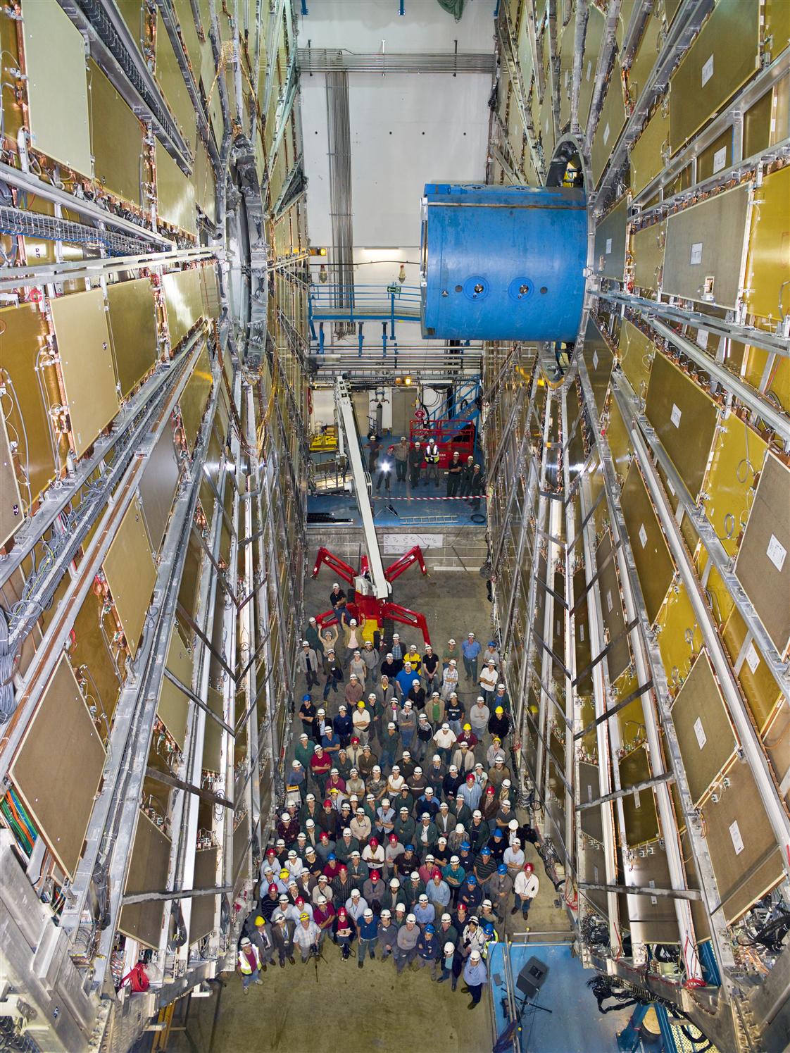
ATLAS celebrates installing the last of the eight big wheels


Source:

The ATLAS end-cap muon detectors, the ‘big wheels’, have been compared to many things: flowers, orange halves, clock faces and works of art. But, more importantly, each is an incredible feat of engineering. On Friday last week the team celebrated the completion of the last wheel, and moved into the final stages of installation.
"I must admit that at the end of last year I would not have believed that we would manage to install these eight big wheels essentially on schedule," admitted Peter Jenni, ATLAS spokesperson. The first of the wheels took a long time to install, but the last one took just a couple of weeks. "This is really a great achievement."
The big wheels harbour ATLAS’s middle layer of muon chambers in the forward region and are one of the last large pieces to be installed. Each is 25m across, weighs between 40 and 50 tonnes and contains around 80 precision chambers or 200 trigger chambers. The support structure itself is just one third of the weight of the total wheel.
Because of their sheer size, each wheel had to be made in 12 pieces for the trigger planes and 16 pieces for the precision-measurement planes, or "petals", of aluminium, the last of which was installed on Friday. Each was assembled at CERN using components from all over the world before being fitted together, piece by piece like a jigsaw.
Because of the need for space for the chambers, designing a suitable structure presented a unique challenge, one that project engineers, Raphaël Vuillermet, Dimitar Mladenov and Giancarlo Spigo were happy to take on.
"The detectors themselves have been on drawings for 15 years; everyone knew where they would go but no one knew about the structure," explains Dimitar. "There were chambers everywhere so our design had to build around them and in the small spaces in between them."
The result after 3 years of calculation, design and sleepless nights was a uniquely thin and light structure that is precise to less than a millimetre.
The 100-member collaboration from Israel, Japan, the US, China, Russia, Europe and Pakistan began assembly of components in 2005 and installation in 2006. "Because the pieces are so delicate we had to be careful throughout the whole process," explains Raphaël. "I was very afraid about something happening to the chambers and also to the people, because you are working 30 metres up. But we didn’t have any problems."
The completion of the big wheels is symbolic for ATLAS because, as technical coordinator Marzio Nessi explains, "the big wheels were always seen as something we would do at the end. And now we have done them."
For Dimitar the biggest challenge was the timing. "I feel proud, but not for myself, for everyone. It was the result of hard work. The only thing that we were lucky about was the weather; if there had been a single day of heavy rain we might have been delayed. But Marzio said not to worry and to leave the weather to him, and the weather was great. I don’t know how he did it!"
Now just two smaller scale wheels and the end-wall chambers remain to be installed, and the big wheels have already begun to give read-outs as part of test runs using cosmic ray data that ATLAS performs every six weeks.
With their striking symmetry and aesthetic appeal the big wheels are likely to become icons of the experiment. But to Marzio, all pieces of ATLAS are beautiful. "This piece just happens to be 25m high."
Fausto Intilla

sabato 13 ottobre 2007

New Path For Designing Novel Nanomaterials Discovered


Source:

Science Daily — A University of Arkansas researcher and his colleagues have found a novel way to “look” at atomic orbitals, and have directly shown for the first time that they change substantially when interacting at the interface of a ferromagnet and a high-temperature superconductor.
This finding opens up a new way of designing nanoscale superconducting materials and fundamentally changes scientific convention, which suggests that only electron spin and atomic charge – not atomic orbitals – influence the properties of superconducting nanostructures. It also has implications for interfaces between other complex oxide materials.
Jacques Chakhalian, assistant professor of physics in the J. William Fulbright College of Arts and Sciences, and his colleagues will publish their findings online at the Science Express Web site, published by the journal Science, Oct. 11.
Until now, materials science researchers believed that an electron’s charge and spin influenced the characteristics of conventional bulk materials. Atomic orbitals, which consist of the patterns of electron density that may be formed in an atom, were previously thought to be inactive.
“In conventional materials like copper or silicon, you could account for everything you could see through charge and spin,” Chakhalian said. Further, orbitals have proved difficult to “see” through physical experimentation, so it wasn’t possible to examine any changes in orbital symmetry that might be taking place at the interface.
Chakhalian’s work has focused on what happens at the interface between two different materials – for instance, superconductors and ferromagnets, two materials with properties that were thought to be incompatible with each other in bulk. In 2006, he and his colleagues created the first high-quality material to have both superconducting and ferromagnetic properties, and they used that material in this experiment.
Chakhalian and his colleagues worked with synchrotron radiation at the Advanced Photon Source, Argonne National Laboratory in Argonne, Ill., to examine the interface between a high-temperature superconducting material containing copper oxide and a ferromagnetic material containing manganese oxide. The synchrotron light is electromagnetic radiation of varying wavelengths that can be tuned to a specific wavelength and polarization for a particular experiment. Unlike conventional X-rays, which diffuse through space, the synchrotron light beams are sharply focused, like a laser beam with extreme brilliance.
The researchers forced the two materials into unusual quantum states. Using a technique called resonant X-ray absorption, they were able to “look” at the atomic orbitals at the interface and determine their symmetry in a non-destructive way.
They found that the atomic orbitals changed the nature of their symmetry at the interface and created a covalent bond between the copper and manganese atoms. This bonding does not exist in the bulk of the individual materials
“When you merge these two materials, the atomic orbitals at the interface become important. They start contributing to the electronic properties of the material,” Chakhalian said. “This opens a new way of designing materials. We can design quantum materials with engineered physical properties.”
The discovery may allow researchers to manipulate nanoscale superconductivity at the interface – opening the possibility of creating room-temperature semiconductors.
Generators that use superconducting materials generate electricity extremely efficiently, at half the size of conventional generators. General Electric estimates the potential market for superconducting generators to be between $20 billion and $30 billion over the next decade.
Chakhalian’s colleagues include J.W. Freeland and M. van Veenendaal of the Advanced Photon Source, Argonne National Laboratory, Argonne, Ill.; and H.-U. Habermeier, G. Cristiani, G. Khaliullin and B. Keimer of the Max Planck Institute for Solid State Research in Stuttgart, Germany.
Note: This story has been adapted from material provided by University of Arkansas, Fayetteville.

Fausto Intilla
www.oloscience.com

Not Just Science Fiction: 'Electromagnetic Wormhole' Possible, Say Mathematicians


Source:

Science Daily — The team of mathematicians that first created the mathematics behind the "invisibility cloak" announced by physicists last October has now shown that the same technology could be used to generate an "electromagnetic wormhole."
In the study, which is to appear in the Oct. 12 issue of Physical Review Letters, Allan Greenleaf, professor of mathematics at the University of Rochester, and his coauthors lay out a variation on the theme of cloaking. Their results open the possibility of building a sort of invisible tunnel between two points in space.
"Imagine wrapping Harry Potter's invisibility cloak around a tube," says Greenleaf. "If the material is designed according to our specifications, you could pass an object into one end, watch it disappear as it traveled the length of the tunnel, and then see it reappear out the other end."
Current technology can create objects invisible only to microwave radiation, but the mathematical theory allows for the wormhole effect for electromagnetic waves of all frequencies. With this in mind, Greenleaf and his coauthors propose several possible applications. Endoscopic surgeries where the surgeon is guided by MRI imaging are problematical because the intense magnetic fields generated by the MRI scanner affect the surgeon's tools, and the tools can distort the MRI images. Greenleaf says, however, that passing the tools through an EM wormhole could effectively hide them from the fields, allowing only their tips to be "visible" at work.
To create cloaking technology, Greenleaf and his collaborators use theoretical mathematics to design a device to guide the electromagnetic waves in a useful way. Researchers could then use these blueprints to create layers of specially engineered, light-bending, composite materials called metamaterials.
Last year, David R. Smith, professor of electrical and computer engineering at Duke's Pratt School, and his coauthors engineered an invisibility device as a disk, which allowed microwaves to pass around it. Greenleaf and his coauthors have now employed more elaborate geometry to specify exactly what properties are demanded of a wormhole's metamaterial in order to create the "invisible tunnel" effect. They also calculated what additional optical effects would occur if the inside of the wormhole was coated with a variety of hypothetical metamaterials.
Assuming that your vision was limited to the few frequencies at which the wormhole operates, looking in one end, you'd see a distorted view out the other end, according the simulations by Greenleaf and his coauthors. Depending on the length of the tube and how often the light bounced around inside, you might see just a fisheye view out the other end, or you might see an Escher-like jumble.
Greenleaf and his coauthors speculated on one use of the electromagnetic wormhole that sounds like something out of science fiction. If the metamaterials making up the tube were able to bend all wavelengths of visible light, they could be used to make a 3D television display. Imagine thousands of thin wormholes sticking up out of a box like a tuft of long grass in a vase. The wormholes themselves would be invisible, but their ends could transmit light carried up from below. It would be as if thousands of pixels were simply floating in the air.
But that idea, Greenleaf concedes, is a very long way off. Even though the mathematics now says that it's possible, it's up to engineers to apply these results to create a working prototype.
Greenleaf's coauthors are Matti Lassas, professor of mathematics at the Helsinki University of Technology; Yaroslav Kurylev, professor of mathematics at the University College, London; and Gunther Uhlmann, Walker Family Endowed Professor of Mathematics at the University of Washington.
Note: This story has been adapted from material provided by University of Rochester.

Fausto Intilla

Quantum Mechanics Predicts Unusual Lattice Dynamics Of Vanadium Metal Under Pressure

Source:

Science Daily — A Swedish research team of Dr. Wei Luo & Professor Rajeev Ahuja and US team of Dr. Y. Ding & Prof. H.K. Mao have used theoretical calculations to understand a totally new type of high-pressure structural phase transition in Vanadium. This phase was not found in earlier experiments for any element and compound. These findings are being published in the Proceedings of the National Academy of Science.
The relation between electronic structure and the crystallographic atomic arrangement is one of the fundamental questions in physics, geophysics and chemistry. Since the discovery of the atomic nature of matter and its periodic structure, this has remained as one of the main questions regarding the very foundation of solid systems.
Scientists at Carnegie's Geophysical Laboratory, USA and Uppsala University, Sweden have discovered a new type of phase transition - a change from one form to another-in vanadium, a metal that is commonly added to steel to make it harder and more durable. Under extremely high pressures, pure vanadium crystals change their shape but do not take up less space as a result, unlike most other elements that undergo phase transitions. This work was appeared in the February 23, 2007 issue of Physical Review Letters.
Trying to understand why high-pressure vanadium uniquely has the record-high superconducting temperature of all known elements inspired us to study high-pressure structure of vanadium. Usually high superconductivity is directly linked to the lattice dynamics of material.
In present paper in PNAS, again a collaboration between Uppsala University and Carnegie's Geophysical Laboratory, USA, we have looked in to the lattice dynamics of vanadium metal and it shows a very unusual behavior under pressure.
A huge change in the electronic structure is driving force behind this unusual lattice dynamics. Moreover, our findings provide a new explanation for the continuous rising of superconducting temperature in high-pressure vanadium, and could lead us to the next breakthrough in superconducting materials.
Note: This story has been adapted from material provided by Uppsala University.

Fausto Intilla
www.oloscience.com

giovedì 11 ottobre 2007

Storing Data On Atomic Roundabouts

Source:
Science Daily — There are right-handed and left-handed yoghurts, right-handed and left-handed snail shells, and right-handed and (occasionally) left-handed screws. Scientists at the University of Bonn have now demonstrated the existence of right-handed and left-handed "magnetic vortices". Through their research, in collaboration with colleagues from Berlin and Geneva, they believe that this physical phenomenon could eventually lead to the construction of faster and more reliable hard disks. The physicists have reported their discovery in Nature.
The magnetic vortex can be pictured like a traffic roundabout. But instead of cars circulating, it consists of an arrangement of magnetised atoms. They form a pattern rather like a ring of tiny bar magnets, so nothing actually moves around the atomic roundabout, but the direction can change: when the "north poles" are all pointing clockwise the magnetic vortex is "right-handed", otherwise the vortex is "left-handed".
"The existence of a circular atomic traffic system of this sort has been presumed for several years," explains the Bonn physics professor Dr. Manfred Fiebig. "In the Nature study we have actually discovered this kind of vortex field in a substance called lithium cobalt phosphate and employed laser-optics to determine its direction." Borrowing from the term "ferromagnetism", the authors -- who include, alongside Manfred Fiebig, the Dutch scientist Bas Van Aken and the Geneva-based physicists Hans Schmid and Jean-Pierre Rivera -- have called the phenomenon "ferrotoroidicity".
This finding is extremely interesting from a fundamental research standpoint. But there could also be very practical consequences in terms of technological applications. This is because magnetic vortices could be used to store information: when the atomic roundabout "traffic" goes right, it could be made to stand for the binary number "0"; going left, it could designate the "1" -- a physical principle that might be introduced one day into the design of computer hard disks.
Slow magnetic fields
"We now store data by magnetically poling the surface coating of a hard disk," explains Manfred Fiebig. "Today's data storage device contains many billions of polable zones, ordered in rows. To write information onto them or read from them you have to have magnetic fields." The current technology has two problems: on the one hand, to produce the necessary fields there must be a flow of electricity for which electrical charge carriers are actuated, and this is a relatively slow process. On the other hand, with ever greater densities of data the danger is that the magnetic fields to be read can destroy the stored information.
The atomic roundabouts do not have these drawbacks. Here, information is also "magnetically" stored but, as Manfred Fiebig points out, the "direction of rotation of the vortices can be changed by electrical fields." Moreover, "The reading process does not require a magnet field that might overwrite the stored data by mistake." Another advantage is that no electricity has to flow to generate the electrical fields so, in principle, storage can run much faster.
Next goal: learning to write
Professor Fiebig came to Bonn University from the Max Born Institute in Berlin over a year ago. The measurements made in Berlin were then analysed in Bonn, and this analysis of the data has produced the proof of the vortices. "We haven't yet succeeded in reading the direction of rotation of the magnetic vortex," the physicist adds. One of the next steps for him and his team is to find out how to write information reliably. They are also looking for other material that may prove suitable for future mass storage media.
However, Fiebig and his team certainly won't be building the hard disk drives of the future as he himself makes clear: "Our primary interest centres on the principles at work behind this phenomenon and what they reveal about the nature of magnetism. But if this research does result one day in a technological application, that'll obviously be quite a bonus."
This study is published in Nature, 11.10.2007, doi: 10.1038/nature06139
Note: This story has been adapted from material provided by University of Bonn.

Fausto Intilla
www.oloscience.com

Light Shed On Light-emitting Nanodevice

Source:
Science Daily — An interdisciplinary team of Cornell nanotechnology researchers has unraveled some of the fundamental physics of a material that holds promise for light-emitting, flexible semiconductors.
The discovery, which involved years of perfecting a technique for building a specific type of light-emitting device, is reported in the journal Nature Materials.*
The interdisciplinary team had long studied the molecular semiconductor ruthenium tris-bipyridine. For many reasons, including its ability to allow electrons and holes (spaces where electrons were before they moved) to pass through it easily, the material has the potential to be used for flexible light-emitting devices. Sensing, microscopy and flat-panel displays are among its possible applications.
The researchers set out to understand the fundamental physics of the material -- that is, what happens when it encounters an electric field, both at the interfaces and inside the film. By fabricating a device out of the ruthenium metal complex that was spin-coated onto an insulating substrate with pre-patterned gold electrodes, the scientists were able to use electron force microscopy to measure directly the electric field of the device.
A long-standing question, according to George G. Malliaras, associate professor of materials science and engineering, director of the Cornell NanoScale Science and Technology Facility and one of the co-principal investigators, was whether an electric field, when applied to the material, is concentrated at the interfaces or in the bulk of the film.
The researchers discovered that it was at the interfaces -- two gold metal electrodes sandwiching the ruthenium complex film -- which was a huge step forward in knowing how to build and engineer future devices.
"So when you apply the electric field, ions in the material move about, and that creates the electric fields at the interfaces," Malliaras explained.
Essential to the effort was the ability to pattern the ruthenium complex using photolithography, a technique not normally used with such materials and one that took the researchers more than three years to perfect, using the knowledge of experts in nanofabrication, materials and chemistry.
The patterning worked by laying down a gold electrode and a polymer called parylene. By depositing the ruthenium complex on top of the parylene layer and filling in an etched gap between the gold electrodes, the researchers were then able to peel the parylene material off mechanically, leaving a perfect device.
Ruthenium tris-bipyridine has energy levels well suited for efficient light emission of about 600 nanometers, said Héctor D. Abruña, the E.M. Chamot Professor of Chemistry, and a principal co-investigator. The material, which has interested scientists for many years, is ideal for its stability in multiple states of oxidation, which, in turn, allows it to serve as a good electron and hole transporter. This means that a single-layer device can be made, simplifying the manufacturing process.
"It's not fabulous, but it has a reasonable emission efficiency," Abruña said. "One of the drawbacks is it has certain instabilities, but we have managed to mitigate most of them."
Among the other authors were co-principal investigators Harold G. Craighead, the C.W. Lake Jr. Professor of Engineering, and John A. Marohn, associate professor of chemistry and chemical biology.
*September 30
Note: This story has been adapted from material provided by Cornell University.

Fausto Intilla
www.oloscience.com

mercoledì 10 ottobre 2007

Unveiling The Structure Of Microcrystals


Source:

Science Daily — Microcrystals take the form of tiny grains, so small that they resemble a powder. How can we determine their structure?
Until now, the technique of X-ray diffraction, normally used to study crystals, was not an appropriate solution. For the first time, researchers from the ESRF and the CNRS have used X-ray diffraction to determine the structure of microcrystal grains of only one cubic micrometre in size.
They gained a factor of a thousand on the size of the analysable samples thanks to new equipment created at the ESRF. This breakthrough opens up new possibilities of research to chemists, physicists and biologists.
The properties of a crystal are determined by the arrangement of its atom in space, its crystalline structure. Scientists use X-ray or neutron diffraction to study crystalline structure when the size of the crystal is more than 10 cubic micrometres. Below this limit, the solid material is considered a powder.
Scientists can apply powder diffraction to analyse such a material but this technique is not easy to exploit. Moreover, powder diffraction can only be used for materials with grain sizes of less than three millionths of a cubic micrometre. Due to these limitations, a determination of the structure of new synthetic solids in powder form is not always possible because the crystals are too small.
The teams from the ESRF and the Institute Lavoisier (CNRS/Université de Versailles Saint-Quentin) have used new set-up permitting X-ray diffraction on crystals of a size of one cubic micrometre, a volume a thousand times smaller than that ever attainable before. This new set-up consists of a focusing system for the ESRF beam, coupled with a goniometer, an instrument to position the sample with maximum precision.
The researchers studied the structure of an organic-inorganic hybrid compound (a microporous aluminium carboxylate), which could be used for gas absorption or to encapsulate various organic molecules. This study confirms that the new set-up allows pushing back the limits in crystal dimension accessible to X-ray diffraction.
“It is a revolution: what was considered a powder in the past has become a crystal today. Researchers can now bring forward samples left in their cupboards because the sizes had previously prevented their study. Now they will be able to elucidate the structures of these samples, with potentially great scientific advances on the horizon”, explains Thierry Loiseau, from the Institut Lavoisier.
Reference: A Microdiffraction Set-up for Nanoporous Metal-Organic-Framework-Type Solids. C. Volkringer, D. Popov, T. Loiseau, N. Guillou, G. Férey, M. Haouas, F. Taulelle, C. Mellot-Draznieks, M. Burghammer and C. Riekel, Nature Materials, 6 (2007) 760-4.
Note: This story has been adapted from material provided by European Synchrotron Radiation Facility.

Fausto Intilla
www.oloscience.com

Taming Tiny, Unruly Waves For Nano Optics


Source:

Science Daily — Nanoscale devices present a unique challenge to any optical technology — there’s just not enough room for light to travel in a straight line.
On the nanoscale, energy may be produced by radiating photons of light between two surfaces very close together (sometimes as close as 10 nanometers), smaller than the wavelength of the light. Light behaves much differently on the nanoscale as its wavelength is interrupted, producing unstable waves called evanescent waves. The direction of these unpredictable waves can’t be calculated, so researchers face the daunting task of designing nanotechnologies to work with the tiny, yet potentially useful waves of light.
Researchers at Georgia Tech have discovered a way to predict the behavior of these unruly waves of light during nanoscale radiation heat transfer, opening the door to the design of a spectrum of new nanodevices (or NEMS) and nanotechnologies, including solar thermal energy technologies.
“This discovery gives us the fundamental information to determine things like how far apart plates should be and what size they should be when designing a technology that uses nanoscale radiation heat transfer,” said Zhuomin Zhang, a lead researcher on the project and a professor in the Woodruff School of Mechanical Engineering. “Understanding the behavior of light at this scale is the key to designing technologies to take advantage of the unique capabilities of this phenomenon.”
The Georgia Tech research team set out to study evanescent waves in nanoscale radiation energy transfer (between two very close surfaces at different temperatures by means of thermal radiation). Because the direction of evanescent waves is seemingly unknowable (an imaginary value) in physics terms, Zhang’s group instead decided to follow the direction of the electromagnetic energy flow (also known as a Poynting vector) to predict behavior rather than the direction of the photons.
“We’re using classic electrodynamics to explain the behavior of the waves, not quantum mechanics,” Zhang said. “We’re predicting the energy propagation — and not the actual movement — of the photons.”
The challenge is that electrodynamics work differently on the nanoscale and the Georgia Tech team would need to pinpoint those differences. Planck’s law, a more than 100-year-old theory about how electromagnetic waves radiate, does not apply on the nanoscale due to fact that the space between surfaces is smaller than a wavelength.
The Georgia Tech team observed that instead of normal straight line radiation, the light was bending as protons tunneled through the vacuum in between the two surfaces just nanometers apart. The team also noticed that the evanescent waves were separating during this thermal process, allowing them to visualize and predict the energy path of the waves.
Understanding the behavior of such waves is critical to the design of many devices that use nanotechnology, including near-field thermophotovoltaic systems, nanoscale imaging based on thermal radiation scanning tunneling microscopy and scanning photon-tunneling microscopy, said Zhang.
These findings were featured on the cover of the Oct. 8 issue of Applied Physics Letters.
Note: This story has been adapted from material provided by Georgia Institute of Technology.

Fausto Intilla

Laser Joining Of Solar Cells


Source:

Science Daily — A single solar cell produces a relatively low output – it’s a case of strength in numbers. Tiny strips of metal are used to link cells together. If the laser soldering temperature is too high, the solder joint may fracture. A new system provides automatic temperature regulation.
Teamwork is what matters – even in the case of solar cells: To obtain sufficient power to operate a pocket calculator, parking ticket dispenser or photovoltaic module, sunlight has to be captured simultaneously by an array of cells. They are connected in series using tiny strips of metal known as stringers. Each stringer has to be positioned in precisely the right spot, then its solder coating is melted using a hot electrode.
When the solder sets, it forms a stable bond with the metallic coating on the silicon. The amount of heat induced in the stringer and the silicon depends on the contact between the soldering electrode and the stringer. Applying too much energy causes thermal stress which in the worst case could destroy the solder joint, leaving a break in the electrical circuit that makes the solar module unfit for use.
Researchers at the Fraunhofer Institute for Laser Technology ILT in Aachen have developed a non-contact soldering system in which the temperature is constantly monitored. If the temperature deviates beyond set limits, the system automatically adjusts it to an acceptable value. “Instead of an electrode, we use a laser beam for the soldering operation,” says ILT department head Dr. Arnold Gillner.
“To melt the solder, we pass a laser beam over the solder-coated stringer. An infrared heat camera derives the temperature of the silicon and of the metal strip from real-time measurements of their emitted radiant heat. If the temperature is too high or too low, a feedback control circuit automatically adapts the laser output within milliseconds.” The system is already in use for industrial surface engineering applications. Solar applications could be on the market in a year or so.
The researchers’ next project is to develop a faster, more reliable method of connecting solar cells by means of laser welding. “Whereas soldering only involves melting the solder, in laser welding the stringer itself is melted,” explains Gillner. This means applying more heat than for soldering, but only for a very short time. “Since the laser is only in contact with the materials for a brief instant, only a small amount of energy is transferred to the materials despite the higher temperature – resulting in even fewer heat-induced defects,” he adds.
What complicates the matter is the fact that the stringer has a diameter of about 200 micrometers, whereas the metallic coating on the silicon required to conduct electricity has a thickness of a mere 10 micrometers. The laser beam has to be modulated in such a way that the stringer will melt while leaving the coating on the silicon intact.
Note: This story has been adapted from material provided by Fraunhofer-Gesellschaft.

Fausto Intilla