Visualizzazione post con etichetta physics. Mostra tutti i post

sabato 27 giugno 2009

A scientist of Indian origin has created new ’superatoms’ with magnetic properties for the first time.


London, June 27 (ANI): A team of researchers led by a scientist of Indian origin has created new ’superatoms’ with magnetic properties for the first time, a breakthrough that could be used to make “spintronic devices”, faster computer processors and denser memory storage.
According to a report in New Scientist, the research was led by Shiv Khanna from Virginia Commonwealth University.
Superatoms were discovered in the 1980s when Walter Knight and colleagues at the University of California, Berkeley, found that groups of sodium atoms can share electrons amongst themselves.
The electrons form a collective “supershell” that coats the cluster.
Until now, clusters that copy the magnetic properties of other elements have proved more difficult to design.
Magnetism is caused by the spin of an atom’s electrons, which are arranged in shells, or orbitals, around the atom’s nucleus.
Their net spin determines the strength of the atom’s magnetic “moment,” and because they tend to occur in pairs that cancel each other out, it is the atom’s unpaired electrons that contribute to its magnetic moment.
Unpaired electrons, however, will make an atom, or a superatom, more likely to react with others in an attempt to fill its orbitals and become stable.
As a result, stability and magnetism have long been thought to be mutually exclusive.
A team led by Shiv Khanna at Virginia Commonwealth University has come up with a way around the problem.
Khanna’s team worked out that encapsulating an atom of vanadium in a cage of eight caesium atoms would create a stable supershell of electrons around the entire cluster.
This would prevent the vanadium atom’s unpaired electrons from reacting with other atoms, maintaining its magnetism.
The arrangement would yield a magnetic moment of five Bohr magnetons, which is the same as an atom of manganese.
“What we have done is expand the range of possible magnetic materials,” said Khanna.
Khanna’s magnetic superatoms are only calculations at this point, but he has funding from the Department of Energy to make them a reality.
He hopes the clusters can be used to give researchers a new dimension of control in designing new materials.
For example, stable magnetic clusters could one day be used in new “spintronic” devices, which compute or store information using magnetic moments rather than simply electrical charge.
Encoding data in this way means the devices can be far smaller than those used to make conventional electronic components, potentially providing an overall boost in computing power. (ANI)

A Higgs boson without the mess.

SOURCE

Particle physicists at CERN’s Large Hadron Collider (LHC) hope to discover the Higgs boson amid the froth of particles born from proton-proton collisions. Results in the 19 June Physical Review Letters show that there may be a way to cut through some of that froth. An experiment at Fermilab’s proton-antiproton collider in Illinois has identified a rare process that produces matter from the intense field of the strong nuclear force but leaves the proton and antiproton intact. There’s a chance the same basic interaction could give LHC physicists a cleaner look at the Higgs.
A proton is always surrounded by a swarm of ghostly virtual photons and gluons associated with the fields of the electromagnetic and strong nuclear forces. Researchers have predicted that when two protons (or a proton and an antiproton) fly past one another at close range, within about a proton’s diameter, these virtual particle clouds may occasionally interact to create new, real (not virtual) particles. The original protons would merely lose some momentum and separate from the beam. Such an “exclusive” reaction–where the original particles don’t break apart–gives unusually clean data because there are so few particles to detect.
In the new experiment, researchers were looking for signs that the interaction of virtual gluons had generated short-lived particles including the Χc (”Chi-c”) and J/ψ mesons, which are charm-anticharm quark pairs that decay into muons and antimuons. The Χc reaction would be especially rare because it requires protons to donate two gluons each, a requirement that also makes detailed predictions challenging, says Fermilab’s Mike Albrow, a member of the Collider Detector at Fermilab (CDF) collaboration.
In 2007, CDF researchers observed hints of exclusive, virtual gluon reactions in the form of high-energy photons radiating from colliding protons and antiprotons. Now the team has sifted through nearly 500 muon-antimuon pairs, identifying 65 that must have come from the decay of the Χc–very close to the rate predicted in 2005 by a team at Durham University in England. Because the Χc has similar particle properties to the much heavier Higgs boson, the same basic reaction should produce the Higgs at the higher collision energies provided by the LHC, says Albrow. “It’s the strongest evidence that the Higgs boson must be produced this way, if it does exist.”
Based on the rate of Χc production, Albrow estimates LHC collisions could produce 100 to 1000 Higgs bosons per year in each of the accelerator’s two largest particle detectors, ATLAS and CMS. “Even a few dozen events per year would enable you to measure the [Higgs's] mass, spin, and other properties,” he says. That’s why ATLAS and CMS teams are reviewing proposals to add detectors to look for exclusive Higgs events.
But not everyone is so optimistic that these events would be detectable in significant numbers. “It looks hard, but one should never say never,” says Joseph Incandela of the University of California, Santa Barbara, deputy physics coordinator for CMS. Incandela points out that once the LHC is operating at full capacity, every crossing of its twin proton beams is expected to yield about 20 collisions, throwing up other particles that may obscure exclusive reactions. But he says there are scenarios such as supersymmetry, a proposed extension to the standard model (the textbook theory of particle physics) in which there could be multiple Higgs bosons. In those situations, Albrow adds, exclusive reactions might be the only ones clean enough to distinguish the different Higgs particles.
by JR Minkel
JR Minkel is a freelance science writer in Nashville, Tennessee. His first book, Instant Egghead Guide: The Universe, comes out in July.
This story was first published in Physical Review Focus and is copyright American Physical Society. Reprinted with permission.
For more information on exclusive events, see the CERN Courier.

lunedì 22 giugno 2009

Chemists Form World's Smallest Droplet Of Acid

SOURCE

ScienceDaily (June 22, 2009) — Exactly four water molecules and one hydrogen chloride molecule are necessary to form the smallest droplet of acid. This was the result of work by the groups of Prof. Dr. Martina Havenith (physical chemistry) and Prof. Dr. Dominik Marx (theoretical chemistry) within the research group FOR 618. They have carried out experiments at ultracold temperatures close to absolute zero temperature using infrared laser spectroscopy to monitor the molecules.
This has been accompanied by theoretical ab initio simulations. According to their calculations, the reaction at these extremely cold temperatures is only possible if the molecules are aggregating one after the other.
Chemistry at ultracold temperatures in space
If you put a classical acid, for example hydrogen chloride in water, the acid molecules will preferentially lose a proton (H+). Thereby the pH-value of the solution is decreased and the solution becomes acidic. In particular, so-called hydronium ions (H3O+), are formed by protonated water molecules. This hydronium ion is an important ingredient in many chemical reactions. Despite of the fact that this is one of the most fundamental reactions, it was not clear until now how many water molecules are actually required in order to form a charge separated negative Cl- ion and a positive H3O+ ion. “Whereas we all know acids from our daily life, we have now been able to observe for the first time acid formation on a molecular level.” "We will need this knowledge in order to understant chemical processes on nanoscopic structures, on small particles and on surfaces” explains Prof. Havenith-Newen. This indicates that there is a rich chemistry even at very low temperatures; a fundamental basis for reactions within stratospheric clouds or in interstellar media. Previously, it had been unclear whether reactions with only a few water molecules can take place at theses ultracold temperatures.
Ultracold trap
For their experiments, the researchers have successively embedded hydrogen chloride as well as single water molecules in a special ultracold trap. They used nanodroplets of suprafluid helium which have a temperature of less than -272,8 °C. Molecules will first be cooled down before they have a chance to aggregate. “Suprafluid” is a special property of the helium which implies that the embedded molecules are still free to rotate before they are frozen, thereby allowing monitoring with unsurpassed precision. Captured in such a way, it is possible to obtain the chemical fingerprint of the acid – its infrared spectrum. By combining trapping with high resolution IR laser spectroscopy and theoretical calculations, the chemists demonstrated that exactly four water molecules are required to form the smallest droplet of acid: (H3O)+(H2O)3Cl-.
Important: One molecule after the other
After these results, the researchers were left with the question of how this reaction can take place at ultracold temperatures near absolute zero. “Usually, activation of chemical reactions requires the input of energy, just like for cooking at home you need a cooking plate or a gas flame” explains Prof. Marx. “However, how should this be possible at a few Kelvin (close to absolute zero)?” The calculations, in combination with experiment, showed that the reaction is only possible by a successive aggregation process. Instead of putting together 4 water molecules and an HCl molecule simultanesously at the beginning and the waiting for a dissociation process to occur, they found in their simulations that when adding the water molecules step by step, a proton is transferred exactly when adding the fourth water molecule. Then, a hydronium ion will immediately form with one of the four added water molecules. This unusual mechanism is called “aggregation induced dissociation”. “We suspect that such aggregation induced reactions, can explain chemical transformations at ultracold conditions, such as can be found at small ice particles in clouds and in interstellar media”, explains Prof. Marx.
The work which described here is part of the research unit FOR 618 “Understanding the Aggregation of Small Molecules with Precise Methods - Interplay between Experiment and Theory”( Co-ordinator: Prof. Dr. Wolfram Sander (Faculty of Chemistry and Biochemistry) which has been funded by the Germany Science Foundation and which has just been extended for three more years after successful evaluation.
Journal reference:
Anna Gutberlet, et al. Below 1 K: The Smallest Droplet of Acid Aggregation-Induced Dissociation of HCl(H2O)4. Science, 324, 1545 (2009) DOI: 10.1126/science.1171753
Adapted from materials provided by Ruhr-Universitaet-Bochum, via AlphaGalileo.

sabato 20 giugno 2009

'Look Mom No Electricity': Transmitting Information with Chemistry


Burning an infofuse transmits a sequence of pulses of light, in which information is encoded using different wavelengths (determined by various metallic salts) and the order of the pattern. Image credit: Samuel W. Thomas III, et al. ©2009 PNAS.
(PhysOrg.com) -- While information technology is generally thought to require electrons or photons for transmitting information, scientists have recently demonstrated a third method of transmission: chemical reactions. Based on a flammable “infofuse,” the new system combines information technology and chemistry into a new area the researchers call "infochemistry."
In the study, led by George Whitesides of Harvard University, with other coauthors from Harvard, Tufts University, and DARPA, the scientists explain that their system transmits in the form of coded pulses of light generated entirely by , without electricity. The system is self-powered, with power being generated by combustion. The power density of the system is higher than that of electrochemical batteries, and has the advantage of not discharging over time.
As Whitesides explained to PhysOrg.com, the significance of the study is that it “demonstrates direct chemical to binary encoding, and transmission of information at a useful bit rate, without batteries.” The researchers hope that their prototype will one day make it possible to make systems that transmit useful information in circumstances in which electronics and batteries do not work, such as harsh environments and under water.
As the scientists explain, the system consists of a strip or fuse of combustible material (nitrocellulose) about 1 mm long. When ignited, a yellow-orange flame moves along the infofuse. To encode information, the scientists patterned the fuse with various metallic salts, which could be done using a desktop inkjet printer or a micropipettor. With their different emission wavelengths, the salts created distinct emission lines in different regions of the , similar to how the colors of fireworks are made: blue (copper), green (barium), yellow (sodium), red (lithium, strontium, calcium), or near-infrared (potassium, rubidium, cesium).
The infofuse, which burns at about 3-4 cm/sec depending on thickness and pattern spacing, is then read by a detector, such as a color CCD camera or fiber optic cable coupled to a spectrometer. The distance between the detector and burning infofuse was typically 2 m, but the detector could still detect a signal up to 30 m away in daylight.
By coding letters of the alphabet using patterns of metallic salts, the scientists transmitted the phrase, “LOOK MOM NO ELECTRICITY” on a single infofuse using the new technique. As the scientists explain, light pulses have several controllable variables that can be used to represent different letters and symbols. In addition to emission wavelength, other variables include pulse duration, time between pulses, and emission intensity. Using combinations of three alkali metals, the researchers demonstrated how to encode 40 different characters by varying some of these parameters.
“It needs a flame, but it does not need additional batteries or power, or auxiliary devices, to convert a chemical signal to a digital one,” Whitesides said. “The power needed to generate the light is produced by chemistry directly, not by drawing power from a battery.”
Although the current infofuses convert energy into light with only 1% of the efficiency of a battery-operated LED, the infofuses generate 10 times more energy per weight than an alkaline battery generates. In general, integrating and chemistry could have certain advantages, possibly leading to systems that operate beyond binary schemes by using a variety of parameters that allow each information unit to carry more information than a bit. Also, since infochemistry is not bound by the principles of electronics (such as fixed circuitry), but rather the principles of chemistry, new systems could lead to novel architectures.
The scientists hope that further improvements to their system could lead to lightweight, portable, self-powered systems that can transmit information and integrate with modern information technologies. Applications could include environmental sensing and transmitting the data optically over a distance. The system could also be used for message transmission in search-and-rescue type applications.
More information: “Infochemistry and infofuses for the chemical storage and transmission of coded information.” Samuel W. Thomas III, et al. Proceedings of the National Academy of Sciences. vol. 106, no. 23, 9147-9150.

venerdì 19 giugno 2009

Scientist Finds Plumber's Wonderland On Graphene

SOURCE

ScienceDaily (June 18, 2009) — Engineers from the University of Pennsylvania, Sandia National Laboratories and Rice University have demonstrated the formation of interconnected carbon nanostructures on graphene substrate in a simple assembly process that involves heating few-layer graphene sheets to sublimation using electric current that may eventually lead to a new paradigm for building integrated carbon-based devices.
Curvy nanostructures such as carbon nanotubes and fullerenes have extraordinary properties but are extremely challenging to pick up, handle and assemble into devices after synthesis. Penn materials scientist Ju Li and Sandia scientist Jianyu Huang have come up with a novel idea to construct curvy nanostructures directly integrated on graphene, taking advantage of the fact that graphene, an atomically thin two-dimensional sheet, bends easily after open edges have been cut on it, which can then fuse with other open edges permanently, like a plumber connecting metal fittings.
The "knife" and "welding torch" used in the experiments, which were performed inside an electron microscope, was electrical current from a Nanofactory scanning probe, generating up to 2000°C of heat. Upon applying the electrical current to few-layer graphene, they observed the in situ creation of many interconnected, curved carbon nanostructures, such as "fractional nanotube"-like graphene bi-layer edges, or BLEs; BLE rings on graphene equivalent to "anti quantum-dots"; and nanotube-BLE assembly connecting multiple layers of graphene.
Remarkably, researchers observed that more than 99 percent of the graphene edges formed during sublimation were curved BLEs rather than flat monolayer edges, indicating that BLEs are the stable edges in graphene, in agreement with predictions based on symmetry considerations and energetic calculations. Theory also predicts these BLEs, or "fractional nanotubes," possess novel properties of their own and may find applications in devices.
Li and Huang observed the creation of these interconnected carbon nanostructures using the heat of electric current and a high-resolution transmission electron microscope. The current, once passed through the graphene layers, improved the crystalline quality and surface cleanness of the graphene as well, both important for device fabrication.
The sublimation of few-layer graphene, such as a 10-layer stack, is advantageous over the sublimation of monolayers. In few-layer graphene, layers spontaneously fuse together forming nanostructures on top of one or two electrically conductive, extended, graphene sheets.
During heating, both the flat graphene sheets and the self-wrapping nanostructures that form, like bilayer edges and nanotubes, have unique electronic properties important for device applications. The biggest obstacle for engineers has been wrestling control of the structure and assembly of these nanostructures to best exploit the properties of carbon. The discoveries of self-assembled novel carbon nanostructures may circumvent the hurdle and lead to new approach of graphene-based electronic devices.
Researchers induced the sublimation of multilayer graphene by Joule-heating, making it thermodynamically favorable for the carbon atoms at the edge of the material to escape into the gas phase, leaving freshly exposed edges on the solid graphene. The remaining graphene edges curl and often welded together to form BLEs. Researchers attribute this behavior to nature's driving force to reduce capillary energy, dangling bonds on the open edges of monolayer graphene, at the cost of increased bending energy.
"This study demonstrates it is possible to make and integrate curved nanostructures directly on flat graphene, which is extended and electrically conducting," said Li, associate professor in the Department of Materials Science and Engineering in Penn's School of Engineering and Applied Science. "Furthermore, it demonstrates that multiple graphene sheets can be intentionally interconnected. And the quality of the plumbing is exceptionally high, better than anything people have used for electrical contacts with carbon nanotubes so far. We are currently investigating the fundamental properties of graphene bi-layer edges, BLE rings and nanotube-BLE junctions."
Short movies of the fabrication of these nanostructures can be viewed at http://www.youtube.com/user/MaterialsTheory.
The study is published in the current issue of the journal Proceedings of the National Academy of Sciences. The study was performed by Li and Liang Qi of Penn, Jian Yu Huang and Ping Lu of the Center for Integrated Nanotechnologies at Sandia and Feng Ding and Boris I. Yakobson of the Department of Mechanical Engineering and Materials Science at Rice.
It was supported by the National Science Foundation, the Air Force Office of Scientific Research, the Honda Research Institute, the Department of Energy and the Office of Naval Research.
Adapted from materials provided by University of Pennsylvania.

Most Efficient And Stable Source Of Pure White Light Ever Achieved

SOURCE

ScienceDaily (June 19, 2009) — Researchers are reporting the first use of a fundamentally new approach in the quest to snare the Holy Grail of the lighting industry: An LED (light-emitting diode) — those ultra-efficient, long-lived light sources — that emits pure white light. The new approach yielded what the scientists describe as the most efficient and stable source of pure white light ever achieved. The advance could speed the development of this next-generation technology for improved lighting of homes, offices, displays, and other applications, they say.
Soo Young Park and colleagues note that white LEDs show promise as a brighter, longer-lasting and more energy-efficient light source than conventional lighting, such as incandescent and fluorescent lights, which they may replace in the future. But scientists have had difficulty producing white LEDs that are suitable for practical use. Existing technologies produce tinted shades of white light, require complex components, and become unstable over time.
The researchers describe development of a new, simpler white LED that is the first to achieve stable white light emissions using a single molecule. Their specially engineered molecule combines two light-emitting materials, one orange and one blue, which together produce white light over the entire visible range. In laboratory studies, the scientists showed that light production from an LED using the new molecule was highly efficient and had excellent color stability and reproducibility, features that make it a practical white light source.
Journal reference:
Park et al. A White-Light-Emitting Molecule: Frustrated Energy Transfer between Constituent Emitting Centers. Journal of the American Chemical Society, 2009; 090610145759060 DOI: 10.1021/ja902533f
Adapted from materials provided by American Chemical Society.

venerdì 12 giugno 2009

ATLAS (LHC,CERN) e-News: It’s like déjà-vu all over again

SOURCE

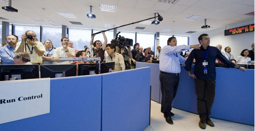
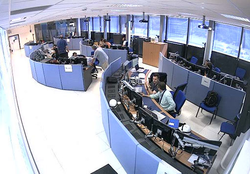
In the movie Groundhog Day, a reporter is forced to re-live a day (February 2) over and over again. Perhaps the coming LHC re-startup would feel like Groundhog Day to some science reporters. CERN therefore has no plans to invite the media here for the first beams this autumn. The first collisions at 450 on 450 GeV (hopefully a short time later) will also be kept low key. What is not fully decided is how to handle the first high-energy collisions and the first events from ATLAS and the other experiments.The images from last September (both control room scenes and the splash events) made a vivid impression on the news media and the public. This time ATLAS will not allow reporters within the Control Room, but the new Visitor Center allows a view of the activities, and new high-quality cameras (mounted on the back wall) can provide the video footage the media wants. The ATLAS website had more than two million hits during the September 2008 activities.Rumors are swirling that Tom Hanks may return to CERN to “turn on” the LHC, but of course that depends on the schedules of Hanks and the LHC. There are several stages in the startup process that could be defined as “turn-on”.Four members of the ATLAS outreach group have been travelling to Sony Pictures (near Hollywood) to help develop a 15-minute CERN/ATLAS “extra” that will be added to the DVD of Angels & Demons that will be released in November. We have also requested to get a copy of the five-minute segment near the beginning of the movie that has some spectacular cinematography of ATLAS. Have you seen our ATLAS webpages on antimatter at http://atlas.ch/angels-demons/ and the new exhibition in the Globe? Finally there have been at least 60 very successful lectures worldwide discussing the science of the movie and the science of LHC.In other news, design work is in progress to replace the aging posters in the Bldg. 40 café. The idea is to make the café an appealing place for physicists to chat and sip coffee, as well as to make it an interesting place to bring visitors to show them the basics of ATLAS.If you haven’t seen modern pop-up books, you will be surprised by the complexity they can portray. ATLAS will soon have its own dramatic pop-up book, a production led by Emma Sanders. It portrays both the detector and the physics.Work is in progress on an animation in the style of the ATLAS animations Episodes I and II. This new project is a joint effort with CMS to portray the physics of the LHC. Two professional animators are working on the project, and a senior person at Pixar has been consulting periodically. Completion date is approximately October 2009. Thought is also being given to an update of the 12-year-old ATLAS movie. All of our videos are on YouTube. Both CERN and ATLAS are working on new/updated communication plans. In the case of CERN, a draft plan has been circulated amongst the experiments. The ATLAS plan is in progress and should be completed in June.These are just the highlights of our activities. You can catch up on the whole series of outreach efforts at the next ATLAS overview week.
Michael Barnett
ATLAS Outreach

ATLAS (LHC,CERN) e-News: Category 1, on shift


SOURCE

To get any physics out of ATLAS, we must manage the data that will course through its cables, from the shifts in the control room to data distribution and software. Christophe Clement, Run Coordinator of ATLAS, describes this important work as less visible since it doesn’t directly result in papers. “And there’s a lot of it,” he adds. “Nevertheless, this is the work that really makes you feel you are carrying out an experiment which has to do with reality.”Control room tasks make up only about 13 per cent of the operation activities, according to Steinar Stapnes, who deals with Operation Task overall planning in ATLAS almost daily, yet they are essential. “Any failure in coverage can have bad consequences, perhaps for hardware and certainly for data taking,” he says.Each institute needs to take its turn on shift; this critical work cannot be compensated for with other contributions that are easier to accomplish remotely or require less diligent attention. For this reason, the Operation Task Planning group has split the operation tasks into two categories: 1 and 2.Category 1 tasks are the real-time operation and monitoring of detector performance, and first line of defence when problems arise, carried out by shifters in the control room and the experts who are called in at anytime of the day or night, should something go wrong. “We make sure that these very important tasks are well-covered. Everybody should feel responsible for them,” says Steinar.He also emphasizes the tradition in particle physics of making sure that graduate students and post-docs get time in the driver’s seat. “For most young people, it’s incredibly interesting, educational, and rewarding for them to get the experience of being part of the team that operates the detector,” says Steinar.Anything beyond the shifts will be Category 2. This includes data acquisition and core software development and maintenance, databases, calibrations, managing data distribution through the Grid, recalibration of data as the detectors are better understood, and software tuning. Category 2 also comprises other tasks associated with processing the data for analysis and those related to longer-term hardware and software maintenance at Point 1.Along with the special designation for shifts and on-call time, the scheduling system has changed. Run Coordination wants to foster a team spirit among the shifters, bringing groups together multiple times over the course of a week. Christophe explained that in this team-based system, shifters: “Get to know the other crew members better, make new contacts, and become more confident with the operation of their sub-detector. Basically work more as a crew.” “It’s not something new in some sense; other experiments have done similar things,” says Steinar, “but it is different with ATLAS because of a larger crew and a large collaboration.”Since collaborators may only work shifts for a maximum of six consecutive days, Run Coordination tried to make a schedule with eight-day blocks, each shifter taking one day off during the block. However, this was in the end deemed too rigid, both for people travelling to CERN to do shifts and for CERN residents. This resulted in a spontaneously generated version with three- and four-day blocks. An unintended consequence was that visiting physicists were inclined to take two blocks in succession, resulting in seven consecutive shifts. CERN safety regulations must be respected, so Run Coordination adjusted the system to allow shifters to choose two consecutive three-day shifts.

This system is also designed to respect the experts who are on-call. In the pattern above, those who work over the weekend have at least a Friday’s worth of experience. This way, the teams are more likely to be able to handle problems without calling in an expert. Christophe notes that on the first day, shifters tend to do some re-learning, but during the rest of a block: “you’ve done this yesterday, and you know what is the problem and how to fix it.”Also, those who take night shift must have recent experience on a day or evening shift, to avoid exhausting the on-call experts with midnight questions and visits to the Control Room. Between the category definitions and block scheduling for shifts, the running of the ATLAS detector should be smooth and effective, with each institution carrying its weight on the front lines.The system starts up Week 26 (28 June to 4 July). For more information or to book a shift, check the webpage.

Katie McAlpine
ATLAS e-News

The element 112, discovered at the GSI (Centre for Heavy Ion Research in Darmstadt)


ScienceDaily (June 12, 2009) — The element 112, discovered at the GSI Helmholtzzentrum für Schwerionenforschung (Centre for Heavy Ion Research) in Darmstadt, has been officially recognized as a new element by the International Union of Pure and Applied Chemistry (IUPAC). IUPAC confirmed the recognition of element 112 in an official letter to the head of the discovering team, Professor Sigurd Hofmann. The letter furthermore asks the discoverers to propose a name for the new element.
Their suggestion will be submitted within the next weeks. In about 6 months, after the proposed name has been thoroughly assessed by IUPAC, the element will receive its official name. The new element is approximately 277 times heavier than hydrogen, making it the heaviest element in the periodic table.
“We are delighted that now the sixth element – and thus all of the elements discovered at GSI during the past 30 years – has been officially recognized. During the next few weeks, the scientists of the discovering team will deliberate on a name for the new element”, says Sigurd Hofmann. 21 scientists from Germany, Finland, Russia and Slovakia were involved in the experiments around the discovery of the new element 112.
Already in 1996, Professor Sigurd Hofmann’s international team created the first atom of element 112 with the accelerator at GSI. In 2002, they were able to produce another atom. Subsequent accelerator experiments at the Japanese RIKEN accelerator facility produced more atoms of element 112, unequivocally confirming GSI’s discovery.
To produce element 112 atoms, scientists accelerate charged zinc atoms – zinc ions for short – with the help of the 120 m long particle accelerator at GSI and “fire” them onto a lead target. The zinc and lead nuclei merge in a nuclear fusion to form the nucleus of the new element. Its so-called atomic number 112, hence the provisional name “element 112”, is the sum of the atomic numbers of the two initial elements: zinc has the atomic number 30 and lead the atomic number 82. An element’s atomic number indicates the number of protons in its nucleus. The neutrons that are also located in the nucleus have no effect on the classification of the element. It is the 112 electrons, which orbit the nucleus, that determine the new element’s chemical properties.
Since 1981, GSI accelerator experiments have yielded the discovery of six chemical elements, which carry the atomic numbers 107 to 112. GSI has already named their officially recognized elements 107 to 111: element 107 is called Bohrium, element 108 Hassium, element 109 Meitnerium, element 110 Darmstadtium, and element 111 is named Roentgenium.
Adapted from materials provided by GSI Helmholtzzentrum für Schwerionenforschung.

martedì 9 giugno 2009

Many Worlds Interpretation (Hugh Everett's Theory) MWI: Testability and Objections

Testability:
Despite the name "interpretation", the MWI is a variant of quantum theory that is different from others. Experimentally, the difference is relative to collapse theories. It seems that there is no experiment distinguishing the MWI from other no-collapse theories such as Bohmian mechanics or other variants of MWI.
The collapse leads to effects that are, in principle, observable; these effects do not exist if the MWI is the correct theory. To observe the collapse we would need a super technology, which allows "undoing" a quantum experiment, including a reversal of the detection process by macroscopic devices. See Lockwood 1989 (p. 223), Vaidman 1998 (p. 257), and other proposals in Deutsch 1986. These proposals are all for gedanken experiments that cannot be performed with current or any foreseen future technology. Indeed, in these experiments an interference of different worlds has to be observed. Worlds are different when at least one macroscopic object is in macroscopically distinguishable states. Thus, what is needed is an interference experiment with a macroscopic body. Today there are interference experiments with larger and larger objects (e.g., fullerene molecules C60), but these objects are still not large enough to be considered "macroscopic". Such experiments can only refine the constraints on the boundary where the collapse might take place. A decisive experiment should involve the interference of states which differ in a macroscopic number of degrees of freedom: an impossible task for today's technology.[8]
The collapse mechanism seems to be in contradiction with basic physical principles such as relativistic covariance, but nevertheless, some ingenious concrete proposals have been made (see Pearle 1986 and the entry on collapse theories). These proposals (and Weissman's 1999 non-linear MW idea) have additional observable effects, such as a tiny energy non-conservation, that were tested in several experiments. The effects were not found and some (but not all!) of these models have been ruled out.
In most no-collapse interpretations, the evolution of the quantum state of the Universe is the same. Still, one might imagine that there is an experiment distinguishing the MWI from another no-collapse interepretation based on the difference in the correspondence between the formalism and the experience (the results of experiments).
An apparent candidate for such an experiment is a setup proposed in Englert et al. 1992 in which a Bohmian world is different from the worlds of the MWI (see also Aharonov and Vaidman 1996). In this example, the Bohmian trajectory of a particle in the past is contrary to the records of seemingly good measuring devices (such trajectories were named surrealistic). However, at present, there are no memory records that can determine unambiguously (without deduction from a particular theory) the particle trajectory in the past. Thus, this difference does not lead to an experimental way of distinguishing between the MWI and Bohmian mechanics. I believe that no other experiment can distinguish between the MWI and other no-collapse theories either, except for some perhaps exotic modifications, e.g., Bohmian mechanics with initial particle position distribution deviating from the quantum distribution. There are other opinions about the possibility of testing the MWI. It has frequently been claimed, e.g. by De Witt 1970, that the MWI is in principle indistinguishable from the ideal collapse theory. On the other hand, Plaga 1997 claims to have a realistic proposal for testing the MWI, and Page 2000 argues that certain cosmological observations might support the MWI.
Objections to the MWI:
Some of the objections to the MWI follow from misinterpretations due to the multitude of various MWIs. The terminology of the MWI can be confusing: "world" is "universe" in Deutsch 1996, while "universe" is "multiverse", etc. There are two very different approaches with the same name "The Many-Minds Interpretation (MMI)". The Albert and Loewer 1988 MMI mentioned above should not be confused with
Lockwood’ 1996 MMI (which resembles the approach of Zeh 1981). The latter is much closer to the MWI as it is presented here, see Sec. 17 of Vaidman 1998. Further, the MWI in the Heisenberg representation (Deutsch 2001) differs significantly from the MWI presented in the Schrödinger representation (used here). The MWI presented here is very close to Everett's original proposal, but in the entry on Everett's relative state formulation of quantum mechanics, as well as in his book Barrett 1999, Barrett uses the name "MWI" for the splitting worlds view publicized by De Witt 1970. This approach has been justly criticized: it has both some kind of collapse (an irreversible splitting of worlds in a preferred basis) and the multitude of worlds. Now I consider the main objections in detail.
Ockham's Razor:
It seems that the majority of the opponents of the MWI reject it because, for them, introducing a very large number of worlds that we do not see is an extreme violation of Ockham's principle: "Entities are not to be multiplied beyond necessity". However, in judging physical theories one could reasonably argue that one should not multiply physical laws beyond necessity either (such a verion of Ockham's Razor has been applied in the past), and in this respect the MWI is the most economical theory. Indeed, it has all the laws of the standard quantum theory, but without the collapse postulate, the most problematic of physical laws. The MWI is also more economic than Bohmian mechanics which has in addition the ontology of the particle trajectories and the laws which give their evolution. Tipler 1986 (p. 208) has presented an effective analogy with the criticism of Copernican theory on the grounds of Ockham's razor.
One might consider also a possible philosophical advantage of the plurality of worlds in the MWI, similar to that claimed by realists about possible worlds, such as Lewis 1986 (see the discussion of the analogy between the MWI and Lewis's theory by Skyrms 1976). However, the analogy is not complete: Lewis' theory considers all logically possible worlds, many more than all worlds incorporated in the quantum state of the Universe.

sabato 6 giugno 2009

Manipulating light on a chip for quantum technologies

SOURCE

An artist's impression of the on-chip quantum metrology experiment (making ultraprecise measurements on chip) Photo by Will Amery, University of Bristol.
(PhysOrg.com) -- A team of physicists and engineers at Bristol University has demonstrated exquisite control of single particles of light — photons — on a silicon chip to make a major advance towards long-sought-after quantum technologies, including super-powerful quantum computers and ultra-precise measurements.
The Bristol Centre for Quantum Photonics has demonstrated precise control of four photons using a microscopic metal electrode lithographically patterned onto a silicon chip.
The photons propagate in silica waveguides — much like in optical fibres — patterned on a silicon chip, and are manipulated with the electrode, resulting in a high-performance miniaturized device.
“We have been able to generate and manipulate of photons on a silicon chip” said PhD student, Jonathan Matthews, who together with Alberto Politi performed the experiments. “These entangled states are responsible for famously ‘weird’ behaviour arising in quantum mechanics, but are also at the heart of powerful quantum technologies.”
“This precise manipulation is a very exciting development for fundamental science as well as for future quantum technologies.” said Prof Jeremy O’Brien, Director of the Centre for Quantum Photonics, who led the research.
The team reports its results in the latest issue of Nature Photonics [June 2009], a sister journal of the leading science journal Nature, and in a Postdeadline Paper at 'The International Quantum Electronics Conference (IQEC)' on June 4 in Baltimore, USA [IQEC Postdeadline Papers].
Quantum technologies with photons
Quantum technologies aim to exploit the unique properties of quantum mechanics, the physics theory that explains how the world works at microscopic scales.
For example a quantum computer relies on the fact that quantum particles, such as photons, can exist in a “superposition” of two states at the same time — in stark contrast to the transistors in a PC which can only be in the state “0” or “1”.
Photons are an excellent choice for quantum technologies because they are relatively noise-free; information can be moved around at the speed of light; and manipulating single photons is easy.
Making two photons “talk” to each other to generate the all-important entangled states is much harder, but Professor O’Brien and his colleagues at the University of Queensland demonstrated this in a quantum logic gate back in 2003 [Nature 426, 264 (2003)].
Last year, the Centre for Quantum Photonics at Bristol showed how such interactions between photons could be realised on a , pointing the way to advanced quantum technologies based on photons [Science 320, 646 (2008)].
Photons are also required to “talk” to each other to realise the ultra-precise measurements that harness the laws of . In 2007 Professor O’Brien and his Japanese collaborators reported such a quantum metrology measurement with four photons [Science 316, 726 (2007)].
Manipulating photons on a silicon chip
“Despite these impressive advances, the ability to manipulate photons on a chip has been missing,” said Mr Politi. “For the last several years the Centre for Quantum Photonics has been working towards building fully functional quantum circuits on a chip to solve these problems,” added Prof O’Brien.
The team coupled photons into and out of the chip, fabricated at CIP Technologies, using optical fibres. Application of a voltage across the metal electrode changed the temperature of the silica waveguide directly beneath it, thereby changing the path that the photons travelled. By measuring the output of the device they confirmed high-performance manipulation of photons in the chip.
The researchers proved that one of the strangest phenomena of the quantum world, namely “quantum entanglement”, was achieved on-chip with up to four photons. Quantum entanglement of two particles means that the state of either of the particles is not defined, but only their collective state, and results in an instantaneous linking of the particles.
This on-chip entanglement has important applications in quantum metrology and the team demonstrated an ultra-precise measurement in this way.
“As well as and quantum metrology, on-chip photonic quantum circuits could have important applications in quantum communication, since they can be easily integrated with optical fibres to send photons between remote locations,” said Alberto Politi.
“The really exciting thing about this result is that it will enable the development of reconfigurable and adaptive quantum circuits for photons. This opens up all kinds of possibilities,” said Prof O’Brien.
A commentary on the work that appeared in the same issue [Nature Photonics 3, 317 (2009)] described it as “an important step in the quest for quantum computation” and concluded: “The most exciting thing about this work is its potential for scalability. The small size of the [device] means that far greater complexity is possible than with large-scale optics.”
The other co-author of the paper is Dr André Stefanov, formerly a Research fellow in the Centre for Quantum Photonics, and now at the Federal Office of Metrology METAS, Switzerland.
Provided by University of Bristol (news : web)

'Colossal' Magnetic Effect Under Pressure


The structure models for F-type and A-type magnetic ordering in manganite in response to pressure. The arrows inside orbitals indicate the spin direction of d electrons.
(PhysOrg.com) -- Millions of people today carry around pocket-sized music players capable of holding thousands of songs, thanks to the discovery 20 years ago of a phenomenon known as the “giant magnetoresistance effect,” which made it possible to pack more data onto smaller and smaller hard drives. Now scientists are on the trail of another phenomenon, called the “colossal magnetoresistance effect” (CMR) which is up to a thousand times more powerful and could trigger another revolution in computing technology.
Understanding, and ultimately controlling, this effect and the intricate coupling between and magnetism in these materials remains a challenge, however, because of competing interactions in manganites, the materials in which CMR was discovered. In the June 12, 2009, issue of the journal Physical Review Letters, a team of researchers report new progress in using high pressure techniques to unravel the subtleties of this coupling.
To study the magnetic properties of manganites, a form of manganese oxide, the research team, led by Yang Ding of the Carnegie Institution’s High Pressure Synergetic Center (HPSync), applied techniques called x-ray magnetic circular dichroism (XMCD) and angular-dispersive diffraction at the (APS) of Argonne National Laboratory in Illinois. High pressure XMCD is a newly developed technique that uses high-brilliance circularly polarized x-rays to probe the magnetic state of a material under pressures of many hundreds of thousands of atmospheres inside a diamond anvil cell.
The discovery of CMR in manganite compounds has already made manganites invaluable components in technological applications. An example is magnetic tunneling junctions in soon-to-be marketed magnetic random access memory (MRAM), where the tunneling of electrical current between two thin layers of manganite material separated by an electrical insulator depends on the relative orientation of magnetization in the manganite layers. Unlike conventional RAM, MRAM could yield instant-on computers. However, no current theories can fully explain the rich physics, including CMR effects, seen in manganites.
“The challenge is that there are competing interactions in manganites among the electrons that determine magnetic properties,” said Ding. “And the properties are also affected by external stimuli, such as, temperature, pressure, magnetic field, and chemical doping.”
“Pressure has a unique ability to tune the electron interactions in a clean and theoretically transparent manner,” he added. “It is a direct and effective means for manipulating the behavior of electrons and could provide valuable information on the magnetic and electronic properties of manganite systems. But of all the effects, pressure effects have been the least explored.”
The researchers found that when a manganite was subjected to conditions above 230,000 times atmospheric pressure it underwent a transition in which its magnetic ordering changed from a ferromagnetic type (electron spins aligned) to an antiferromagnetic type (electron spins opposed). This transition was accompanied by a non-uniform structural distortion called the Jahn-Teller effect.
“It is quite interesting to observe that uniform compression leads to a non-uniform structural change in a manganite, which was not predicted by theory,” said Ding, “Working with Michel van Veenendaal’s theoretical group at APS, we found that the predominant effect of pressure on this material is to increase the strength of an interaction known as superexchange relative to another known as the double exchange interaction. A consequence of this is that the overall ferromagnetic interactions in the system occur in a plane (two dimensions) rather than in three dimensions, which produces a non-uniform redistribution of electrons. This leads to the structural distortion.”
Another intriguing response of manganite to high pressure revealed by the experiments is that the magnetic transition did not occur throughout the sample at the same time. Instead, it spread incrementally.
“The results imply that even at ambient conditions, the manganite might already have two separate magnetic phases at the nanometer scale, with pressure favoring the growth of the antiferro-magnetic phase at the expense of the ferromagnetic phase,” said coauthor Daniel Haskel, a physicist at Argonne’s APS. “Manipulating phase separation at the nanoscale level is at the very core of nanotechnology and manganites provide an excellent playground to pursue this objective”.
“This work not only displays another interesting emergent phenomenon arising from the interplay between charge, spin, orbital and lattice in a strongly correlated electron system,” commented coauthor Dr. Ho-kwang Mao of Carnegie’s Geophysical Laboratory, Director of HPSync,” but it also manifests the role of pressure in magnetism studies of dense matter.”
More information: Pressure-induced magnetic transition in manganite (La0.75Ca0.25MnO3) Yang Ding, Daniel Haskel, Yuan-Chieh Tseng, Eiji Kaneshita, Michel van Veenendaal, John Mitchell, Stanislav V. Sinogeikin, Vitali Prakapenka, and Ho-kwang Mao, Physical Review Letters, June 2009.
Provided by Carnegie Institution

venerdì 5 giugno 2009

Lasers Are Making Solar Cells Competitive

SOURCE

ScienceDaily (June 4, 2009) — Solar electricity has a bright future: It is renewable and available in unlimited quantities, and it does not produce any gases detrimental to the climate. Its only drawback right now is the price: the electric power currently being produced by solar cells in northern Europe must be subsidized if it is to compete against the household electricity generated by traditional power plants. At "Laser 2009" in Munich, June 15 to 18, Fraunhofer researchers will be demonstrating how laser technology can contribute to optimizing the manufacturing costs and efficiency of solar cells.
Cell phones, computers, MP3 players, kitchen stoves, and irons all have one thing in common: They need electricity. And in the future, more and more cars will also be fuelled by electric power. If the latest forecast from the World Energy Council WEC can be believed, global electricity requirements will double in the next 40 years. At the same time, prices for the dwindling resources of petroleum and natural gas are climbing.
“Rising energy prices are making alternative energy sources increasingly cost-effective. Sometime in the coming years, renewable energy sources, such as solar energy, will be competitive, even without subsidization,” explains Dr. Arnold Gillner, head of the microtechnology department at the Fraunhofer Institute for Laser Technology in Aachen, Germany. “Experts predict that grid parity will be achieved in a few years. This means that the costs and opportunities in the grid will be equal for solar electricity and conventionally generated household electricity.” Together with his team at the Fraunhofer Institute for Laser Technology ILT in Aachen, this researcher is developing technologies now that will allow faster, better, and cheaper production of solar cells in the future. “Lasers work quickly, precisely, and without contact. In other words, they are an ideal tool for manufacturing fragile solar cells. In fact, lasers are already being used in production today, but there is still considerable room for process optimization.” In addition to gradually improving the manufacturing technology, the physicists and engineers in Aachen are working with solar cell developers - for example, at the Fraunhofer Institute for Solar Energy Systems ISE in Freiburg - on new engineering and design alternatives.
New production technologies allow new design alternatives
At “Laser 2009” in Munich, the researchers will be demonstrating how lasers can drill holes into silicon cells at breathtaking speed: The ILT laser system drills more than 3,000 holes within one second. Because it is not possible to move the laser source at this speed, the experts have developed optimized manufacturing systems which guide and focuses the light beam at the required points. “We are currently experimenting with various laser sources and optical systems,” Gillner explains. “Our goal is to increase the performance to 10,000 holes a second. This is the speed that must be reached in order to drill 10,000 to 20,000 holes into a wafer within the cycle time of the production machines.”
The tiny holes in the wafer - their diameter is only 50 micrometers – open up undreamt-of possibilities for the solar cell developers. “Previously, the electrical contacts were arranged on the top of the cells. The holes make it possible to move the contacts to the back, with the advantage that the electrodes, which currently act as a dark grid to absorb light, disappear. And so the energy yield increases. The goal is a degree of efficiency of 20 percent% in industrially-produced emitter wrap-through (EWT) cells, with a yield of one-third more than classic silicon cells,” Gillner explains. The design principle itself remains unchanged: In the semi-conductor layer, light particles, or photons, produce negative electrons and positive holes, each of which then wanders to the oppositely poled electrodes. The contacts for anodes and cathodes in the EWT cells are all on the back, there is no shading caused by the electrodes, and the degree of efficiency increases. With this technique, it may one day be possible to use unpurified “dirty” silicon to manufacture solar cells that have poorer electrical properties, but that are cheaper.
Drilling holes into silicon cells is only one of many laser applications in solar cell manufacturing. In the EU project Solasys – Next Generation Solar Cell and Module Laser Processing Systems – an international research team is currently developing new technologies that will allow production to be optimized in the future. ILT in Aachen is coordinating the six million euro project. “We are working on new methods that make the doping of semiconductors, the drilling and the surface structuring of silicon, the edge isolation of the cells, and the soldering of the modules more economical,” project coordinator Gillner explains. For example, “selective laser soldering” makes it possible to improve the rejection rates and quality of the contacting, and so reduce manufacturing costs. Until now, the electrodes were mechanically pressed onto the cells, and then heated in an oven. “But silicon cells often break during this process,” Gillner knows. “Breakage is a primary cost factor in production.” On the other hand, however, with “selective laser soldering” the contacts are pressed on to the cells with compressed air and then soldered with the laser. The mechanical stress approaches zero and the temperature can be precisely regulated. The result: Optimal contacts and almost no rejects.
Laser technology means more efficient thin film cells
Laser technology is also helping to optimize the manufacture of thin film solar cells. The extremely thin film packages made of semiconducting oxide, amorphous silicon, and metal that are deposited onto the glass panels still have a market share of only ten percent. But as Gillner knows, “This could be higher, because thin film solar cells can be used anywhere that non-transparent glass panels can be mounted, for example, on house facades or sound-insulating walls. But the degrees of efficiency are comparable low at five to eight percent, and the production costs are comparatively high.” The laser researchers are working to improve these costs. Until now, the manufacturers have used mechanical methods or solid-state lasers in the nanosecond range in order to structure the active layers on the glass panels. In order to produce electric connections between the semiconductor and the metal, grooves only a few micrometers wide must be created. At the Fraunhofer-Gesellschaft booth at “Laser 2009” the ILT researchers will be demonstrating a 400-watt ultrashort pulse laser that processes thin-film solar modules ten times faster than conventional diode-pumped solid-state lasers. “The ultrashort pulse laser is an ideal tool for ablating thin layers: It works very precisely, does not heat the material and, working with a pulse frequency of 80 MHz, can process a 2-by-3 meter glass panel in under two minutes,” Gillner reports. “The technology is still very new, and high-performance scanning systems and optical systems adapted to the process must be developed first. In the medium term, however, this technology will be able to reduce production costs.”
The rise of laser technology in solar technology is just taking off, and it still has a long way to go. “Lasers simplify and optimize the manufacture of classic silicon and thin-film cells, and they allow the development of new design alternatives,” Gillner continues. “And so laser technology is making an important contribution towards allowing renewable energy sources to penetrate further into the energy market.”
Adapted from materials provided by Fraunhofer-Gesellschaft.

Theorists Reveal Path To True Muonium -- Never-seen Atom

SOURCE

ScienceDaily (June 4, 2009) — True muonium, a long-theorized but never-seen atom, might be observed in future experiments, thanks to recent theoretical work by researchers at the Department of Energy's SLAC National Accelerator Laboratory and Arizona State University. True muonium was first theorized more than 50 years ago, but until now no one had uncovered an unambiguous method by which it could be created and observed.
"We don't usually work in this area, but one day we were idly talking about how experimentalists could create exotic states of matter," said SLAC theorist Stanley Brodsky, who worked with Arizona State's Richard Lebed on the result. "As our conversation progressed, we realized 'Gee…we just figured out how to make true muonium.'"
True muonium is made of a muon and an anti-muon, and is distinguished from what's also been called "muonium"—an atom made of an electron and an anti-muon. Both muons and anti-muons are created frequently in nature when energetic particles from space strike the earth's atmosphere. Yet both have a fleeting existence, and their combination, true muonium, decays naturally into other particles in a few trillionths of a second. This makes observation of the exotic atom quite difficult.
In a paper published this week in Physical Review Letters, Brodsky and Lebed describe two methods by which electron–positron accelerators could detect the signature of true muonium's formation and decay.
In the first method, an accelerator's electron and positron beams are arranged to merge, crossing at a glancing angle. Such a collision would produce a single photon, which would then transform into a single true muonium atom that would be thrown clear of the other particle debris. Because the newly created true muonium atoms would be traveling so fast that the laws of relativity govern, they would decay much slower than they would otherwise, making detection easier. [An artist's impression of this process can be seen at right.]
In the second method, the electron and positron beams collide head-on. This would produce a true muonium atom and a photon, tangled up in a cloud of particle debris. Yet simply by recoiling against each other, the true muonium and the photon would push one another out of the debris cloud, creating a unique signature not previously searched for.
"It's very likely that people have already created true muonium in this second way," Brodsky said. "They just haven't detected it."
In their paper, Lebed and Brodsky also describe a possible, but more difficult, means by which experimentalists could create true tauonium, a bound state of a tau lepton and its antiparticle. The tau was first created at SLAC's SPEAR storage ring, a feat for which SLAC physicist Martin Perl received the 1995 Nobel Prize in physics.
Brodsky attributes the pair's successful work to a confluence of events: various unrelated lectures, conversations and ideas over the years, pieces of which came together suddenly during his conversation with Lebed.
"Once you pull all of the ideas together, you say 'Of course! Why not?' Brodsky said. "That's the process of science—you try to relate everything new to what you already know, creating logical connections."
Now that those logical connections are firmly in place, Brodsky said he hopes that one of the world's colliders will perform the experiments he and Lebed describe, asking, "Who doesn't want to see a new form of matter that no one's ever seen before?"
Journal reference:
Stanley J. Brodsky and Richard F. Lebed. Production of the Smallest QED Atom: True Muonium (µ µ-). Physical Review Letters, 2009; DOI: 10.1103/PhysRevLett.102.213401
Adapted from materials provided by DOE/SLAC National Accelerator Laboratory.

Scientists Demonstrate All-fiber Quantum Logic

SOURCE

ScienceDaily (June 4, 2009) — A team of physicists and engineers have demonstrated all-fiber quantum logic, where single photons are generated and used to perform the contolled-NOT quantum logic gate in optical fibers with high fidelity.
The only quantum technology in practical use today is quantum cryptography and is currently limited in the distance over which secure communication may occur.
More sophisticated quantum networks will require multiple nodes with the ability to implement small-scale quantum processing in order to increase the range of quantum communications. Such networks will rely on optical fiber links, making fiber-based photon generation and information processing of key technological importance.
Jeremy O’Brien, Professor of Physics and Electrical Engineering at Bristol University and colleagues, have shown it is possible for a high-fidelity fiber controlled-NOT gate to operate with fiber heralded single-photon sources.
Professor O’Brien speaking about the research, said: “On the basis of a simple model we are able to conclude that imperfections are primarily due to the photon sources, meaning that the gate itself works with very high fidelity.”
“Such all fiber quantum information processing will likely have important applications in future quantum networks.”
All-fiber quantum information processing could be used in less mature quantum technologies such as computing, communication and advanced measurement, as well as in the fundamental science of quantum optics.
The team reported its results in the March 2009 issue of Physical Review A (Vol 79, No 3).
Journal reference:
Alex S. Clark, Jérémie Fulconis, John G. Rarity, William J. Wadsworth, and Jeremy L. O%u2018Brien. All-optical-fiber polarization-based quantum logic gate. Physical Review A, 2009; 79 (3): 030303 DOI: 10.1103/PhysRevA.79.030303
Adapted from materials provided by University of Bristol.

Goal: Developing The Best Atomic Clock In The World

SOURCE

ScienceDaily (June 5, 2009) — They are masters at working with light: the scientists at the newly founded QUEST Institute at the Physikalisch-Technische Bundesanstalt (PTB), Braunschweig. And they want to work on some of the most exciting questions relating to physics today: on unimaginably precise methods of measurement for observing the Earth, on the pressing question of the fundamentals of physics, of whether the fundamental constants are really constant, and on the development of the best atomic clock in the world made of a single aluminium atom.
These are just some examples from the catalogue of tasks which the scientists have drawn up for themselves. This gives us an idea of why optics is often described as "the" key technology of the 21st century.
QUEST stands for "Quantum Engineering and Space-Time Research" and it is the name of a whole Excellence Cluster to which the new institute belongs. It is already a prime example of good cooperation between completely different but perfectly complementary partners: Next to PTB as the state research institute of the Federal Ministry of Economics (BMWi) with its special knowledge in the field of metrology, i.e. precise measurement technologies, there are six institutes from the Leibniz University of Hannover, the Laser Zentrum Hannover, the German-British Gravitational Wave Detector GEO600 in Ruthe, the Center of Applied Space Technology and Microgravity (ZARM) in Bremen and the Albert Einstein Institute (Max Planck Institute for Gravitational Physics).
Now strengthened once more by the new QUEST Institute at PTB, the joint research is not only to answer the deep fundamental issues of physics, but also to lead to new high tech products with industry. In its start-up phase the institute is being financed by the German Research Foundation (DFG). After this period of funding, the professorship will be permanently continued by PTB and German Federal Ministry of Economics and Technology (BMWI).
A long, intensive search – this is the meaning of the word "quest". A good secondary meaning for the acronym, which primarily came about as the abbreviation of fields of research which previously existed more in parallel. "Quantum Engineering", the first part of the name stands for a relatively new branch of research, which deals with the control of quantum physics at the engineering level. "Space-Time Research", the second part, is research dealing with all aspects of space and time, for example the development of ever more exact atomic clocks or new processes to explore space, for instance precise measurement procedures in geodesy. Because in atomic clocks as well as in novel quantum sensors the main focus is on nothing more than using quantum phenomena with the aid of state-of-the-art technologies, founding the Excellence Cluster QUEST in November 2007 was a success right from the start. For this made it possible to gather the competence of the specialised scientists and institutions in a completely new way and much more intensively.
This success story is now opening another chapter: at PTB, in the immediate vicinity of the unique measuring equipment and some of the best atomic clocks in the world, a new research group has started working: the QUEST Institute at PTB consists of a Professorship ("Experimental Quantum Metrology"), a Junior Research Group ("Cold Ion Quantum Sensors"), a Research Project ("Sub-hertz Lasers and novel optic resonators“) as well as several so-called Task Groups.
Prof. Dr. Piet O. Schmidt, Head of the Institute, specialises in new methods of spectroscopy. "We use, for example, the exactly identical frequency distances of the spectral lines in an optical frequency comb in order to investigate atomic or molecular systems," explains Schmidt. "What is also very interesting are the methods of quantum logic originally developed for future quantum computers with stored ions, but which can also be used for investigating special classes of atoms or molecules which were not spectroscopically accessible or could only be accessed with difficulty previously." He also wants to use the quantum logic spectroscopy to develop an optical atomic clock on the basis of an extremely narrow transition in a single aluminium ion. "There is a chance that it might become the best atomic clock in the world", says Schmidt.
The clock that Schmidt has in mind is to attain a relative uncertainly of 10-18 (to date the limit at PTB lies at 10-15, held by the so-called caesium fountain clocks). The researchers will, thus, be able to pursue more intensively the question of whether the fine-structure constant, the gravitational constant or the mass ratio between the electron and the proton, change in space or time, as predicted by some modern theories in physics such as the String Theory. But concrete measurement capabilities will also be connected to this.
"The availability of such sensitive clocks will lead to other highly sensitive measuring instruments, which will be able to determine, for example, a change in the gravitational potential of the Earth with an accuracy corresponding to a height difference of one centimetre," explains Schmidt. "Currently the geoid of the Earth is known with an uncertainty of 30 cm to 50 cm." With QUEST, interdisciplinary cooperations between engineers who deal with the development of navigation systems, geodesists as well as researchers in the field of laser cooled atoms, are to be stimulated. This is to lead to the development of novel sensors for geoscience and navigation.
And probably the most important characteristic of QUEST lies right here: the intensive cooperation of thematically related but to date organisationally separate research groups: that is between university research, several federal research institutions and an international project on basic research. Not least, the novel quantum engineering technologies will probably also lead to forward-looking cooperations with industrial partners and, thus, to new commercial applications.
Adapted from materials provided by Physikalisch-Technische Bundesanstalt (PTB).

venerdì 29 maggio 2009

Regular Light Bulbs Made Super-Efficient with Ultra-Fast Laser

SOURCE

Chunlei Guo stands in front of his femtosecond laser, which can double the efficiency of a regular incandescent light bulb. Credit: University of Rochester
(PhysOrg.com) -- An ultra-powerful laser can turn regular incandescent light bulbs into power-sippers, say optics researchers at the University of Rochester. The process could make a light as bright as a 100-watt bulb consume less electricity than a 60-watt bulb while remaining far cheaper and radiating a more pleasant light than a fluorescent bulb can.
The laser process creates a unique array of nano- and micro-scale structures on the surface of a regular tungsten filament—the tiny wire inside a light bulb—and theses structures make the tungsten become far more effective at radiating light.
The findings will be published in an upcoming issue of the journal .
"We've been experimenting with the way ultra-fast lasers change metals, and we wondered what would happen if we trained the laser on a filament," says Chunlei Guo, associate professor of optics at the University of Rochester. "We fired the right through the glass of the bulb and altered a small area on the filament. When we lit the bulb, we could actually see this one patch was clearly brighter than the rest of the filament, but there was no change in the bulb's energy usage."
The key to creating the super-filament is an ultra-brief, ultra-intense beam of light called a femtosecond laser pulse. The laser burst lasts only a few quadrillionths of a second. To get a grasp of that kind of speed, consider that a femtosecond is to a second what a second is to about 32 million years. During its brief burst, Guo's laser unleashes as much power as the entire grid of North America onto a spot the size of a needle point. That intense blast forces the surface of the metal to form nanostructures and microstructures that dramatically alter how efficiently can radiate from the filament.
In 2006, Guo and his assistant, Anatoliy Vorobeyv, used a similar laser process to turn any metal pitch black. The surface structures created on the metal were incredibly effective at capturing incoming radiation, such as light.
"There is a very interesting 'take more, give more' law in nature governing the amount of light going in and coming out of a material," says Guo. Since the black metal was extremely good at absorbing light, he and Vorobyev set out to study the reverse process—that the blackened filament would radiate light more effectively as well.
"We knew it should work in theory," says Guo, "but we were still surprised when we turned up the power on this bulb and saw just how much brighter the processed spot was."
In addition to increasing the brightness of a bulb, Guo's process can be used to tune the color of the light as well. In 2008, his team used a similar process to change the color of nearly any metal to blue, golden, and gray, in addition to the black he'd already accomplished. Guo and Vorobeyv used that knowledge of how to control the size and shape of the nanostructures—and thus what colors of light those structures absorb and radiate—to change the amount of each wavelength of light the tungsten filament radiates. Though Guo cannot yet make a simple bulb shine pure blue, for instance, he can change the overall radiated spectrum so that the tungsten, which normally radiates a yellowish light, could radiate a more purely white light.
Guo's team has even been able to make a filament radiate partially polarized light, which until now has been impossible to do without special filters that reduce the bulb's efficiency. By creating nanostructures in tight, parallel rows, some light that emits from the filament becomes polarized.
The team is now working to discover what other aspects of a common light bulb they might be able to control. Fortunately, despite the incredible intensity involved, the femtosecond laser can be powered by a simple wall outlet, meaning that when the process is refined, implementing it to augment regular light bulbs should be relatively simple.
Guo is also announcing this month in Applied Physics Letters a technique using a similar femtosecond process to make a piece of metal automatically move liquid around its surface, even lifting a liquid up against gravity.
Source: University of Rochester (news : web)

World's largest laser opens: We are close to practice the nuclear fusion


Scientists for decades have been hunting for ways to harness the enormous force of the sun and stars to supply energy here on Earth. The National Ignition Facility at the Lawrence Livermore Laboratory may spark the light at the end of the tunnel.
The facility was dedicated today (May 29) at a ceremony attended by numerous state and national officials.
Roughly the size of three football fields, the facility houses the world’s largest laser. Within the next three years, its 192 laser beams will deliver massive amounts of at a pea-sized target. That target, filled with , will in turn release 10 to 100 times the power than the amount injected by the laser.

When all of the lasers’ energy slams the target, it will generate unprecedented temperatures in the target materials - temperatures of more than 100 million degrees and pressures more than 100 billion times the Earth’s atmosphere. These conditions are similar to those in the stars and the cores of . Igniting these conditions will create nuclear fusion, which is the reaction that gives the sun and the stars their immense power. Mimicking and controlling the highly volatile process - tantamount to creating a star in a laboratory - could lead to ways to produce plentiful clean and safe energy.
While demonstrating nuclear fusion as a viable means for abundant clean energy may be the most exciting offshoot of NIF research, another of its roles is to study the conditions associated with the inner workings of nuclear weapons.
The NIF is a cornerstone of a critical national security mission to ensure the reliability and safety of the U.S. nuclear stockpile without conducting underground testing. At NIF, scientists will be able to provide data for supercomputer simulations that replicate conditions that exist inside a thermonuclear weapon.
NIF experiments will also help scientists who are trying to understand the universe in many fundamental ways, including astrophysicists learning about the hot, dense interiors of large planets, stars and other phenomena.
Provided by University of California

Researchers make breakthrough in the quantum control of light


This image represents a quantum state with zero, three and six photons simultaneously. The theory is on left and the experiment is on the right. Image: UCSB.
Researchers at UC Santa Barbara have recently demonstrated a breakthrough in the quantum control of photons, the energy quanta of light. This is a significant result in quantum computation, and could eventually have implications in banking, drug design, and other applications.
In a paper to be published in today's issue of the journal Nature, UCSB physics researchers Max Hofheinz, John Martinis, and Andrew Cleland document how they used a superconducting electronic circuit known as a Josephson phase qubit to prepare highly unusual quantum states using microwave-frequency photons. The breakthrough is the result of four years of work in the laboratories of Cleland and Martinis.
The project is funded by the federal agency called the Intelligence Advanced Research Projects Activity, or IARPA. The government is particularly interested in quantum computing because of the way banking and other important communications are currently encrypted. Using large numbers, with hundreds of digits, encryption codes are changed daily and would take years of traditional computing to break. could potentially break those codes quickly, destroying current encryption schemes.
In the experiments, the photons were stored in a microwave cavity, a "light trap" in which the light bounces back and forth as if between two mirrors. In earlier work, these researchers showed they could create and store photons, one at a time, with up to 15 photons stored at one time in the light trap. The research shows that they can create states in which the light trap simultaneously has different numbers of photons stored in it. For example, it can simultaneously have zero, three, and six photons at the same time. Measuring the by counting how many photons are stored forces the trap to "decide" how many there are; but prior to counting, the light trap exists in a quantum superposition, with all three outcomes possible.
Explaining the paradoxical simultaneity of quantum states, Cleland said that it's like having your cake and eating it -- at the same time.
"These superposition states are a fundamental concept in quantum mechanics, but this is the first time they have been controllably created with light," Cleland said. Martinis added, "This experiment can be thought of as a quantum digital-to-analog converter." As digital-to-analog converters are key components in classical communication devices (for example, producing the sound waveforms in cell phones), this experiment might enable more advanced communication protocols for the transmission of quantum information.
First author Hofheinz designed and performed the measurements. He is a postdoctoral researcher from Germany who has been working at UCSB for the last two years on this project. The devices used to perform the experiment were made by Haohua Wang, a postdoctoral researcher from China, who is second author on the Nature publication.
The scientists said their research is leading to the construction of a quantum computer, which will have applications in information encryption and in solving or simulating problems that are not amenable to solution using standard computers.
Source: University of California - Santa Barbara (news : web)

Theorists Reveal Path to True Muonium


In this artist's depiction of how experimentalists could create true muonium, an electron (blue) and a positron (red) collide, producing a virtual photon (green) and then a muonium atom, made of a muon (small yellow) and an anti-muon (small purple). The muonium atom then decays back into a virtual photon and then a positron and an electron. Overlaying this process is a figure indicating the structure of the muonium atom: one muon (large yellow) and one anti-muon (large purple). Credit: Graphic: Terry Anderson/SLAC
(PhysOrg.com) -- True muonium, a long-theorized but never-seen atom, might be observed in future experiments, thanks to recent theoretical work by researchers at the Department of Energy's SLAC National Accelerator Laboratory and Arizona State University. True muonium was first theorized more than 50 years ago, but until now no one had uncovered an unambiguous method by which it could be created and observed.
"We don't usually work in this area, but one day we were idly talking about how experimentalists could create exotic states of matter," said SLAC theorist Stanley Brodsky, who worked with Arizona State's Richard Lebed on the result. "As our conversation progressed, we realized 'Gee…we just figured out how to make true muonium.'"
True muonium is made of a muon and an anti-muon, and is distinguished from what's also been called "muonium"—an atom made of an electron and an anti-muon. Both muons and anti-muons are created frequently in nature when energetic particles from space strike the earth's atmosphere. Yet both have a fleeting existence, and their combination, true muonium, decays naturally into other particles in a few trillionths of a second. This makes observation of the exotic atom quite difficult.
In a paper published on Tuesday in , Brodsky and Lebed describe two methods by which electron-positron accelerators could detect the signature of true muonium's formation and decay.
In the first method, an accelerator's electron and positron beams are arranged to merge, crossing at a glancing angle. Such a collision would produce a single photon, which would then transform into a single true muonium atom that would be thrown clear of the other particle debris. Because the newly created true muonium atoms would be traveling so fast that the laws of govern, they would decay much slower than they would otherwise, making detection easier.
In the second method, the electron and positron beams collide head-on. This would produce a true muonium atom and a photon, tangled up in a cloud of particle debris. Yet simply by recoiling against each other, the true muonium and the photon would push one another out of the debris cloud, creating a unique signature not previously searched for.
"It's very likely that people have already created true muonium in this second way," Brodsky said. "They just haven't detected it."
In their paper, Lebed and Brodsky also describe a possible, but more difficult, means by which experimentalists could create true tauonium, a bound state of a tau lepton and its antiparticle. The tau was first created at SLAC's SPEAR storage ring, a feat for which SLAC physicist Martin Perl received the 1995 Nobel Prize in physics.
Brodsky attributes the pair's successful work to a confluence of events: various unrelated lectures, conversations and ideas over the years, pieces of which came together suddenly during his conversation with Lebed.
"Once you pull all of the ideas together, you say 'Of course! Why not?' Brodsky said. "That's the process of science—you try to relate everything new to what you already know, creating logical connections."
Now that those logical connections are firmly in place, Brodsky said he hopes that one of the world's colliders will perform the experiments he and Lebed describe, asking, "Who doesn't want to see a new form of matter that no one's ever seen before?"
More information: "Production of the Smallest QED Atom: True Muonium," Physical Review Letters
Source: SLAC National Laboratory (news : web)