Visualizzazione post con etichetta Energy Technology. Mostra tutti i post

sabato 27 giugno 2009

A Higgs boson without the mess.

SOURCE

Particle physicists at CERN’s Large Hadron Collider (LHC) hope to discover the Higgs boson amid the froth of particles born from proton-proton collisions. Results in the 19 June Physical Review Letters show that there may be a way to cut through some of that froth. An experiment at Fermilab’s proton-antiproton collider in Illinois has identified a rare process that produces matter from the intense field of the strong nuclear force but leaves the proton and antiproton intact. There’s a chance the same basic interaction could give LHC physicists a cleaner look at the Higgs.
A proton is always surrounded by a swarm of ghostly virtual photons and gluons associated with the fields of the electromagnetic and strong nuclear forces. Researchers have predicted that when two protons (or a proton and an antiproton) fly past one another at close range, within about a proton’s diameter, these virtual particle clouds may occasionally interact to create new, real (not virtual) particles. The original protons would merely lose some momentum and separate from the beam. Such an “exclusive” reaction–where the original particles don’t break apart–gives unusually clean data because there are so few particles to detect.
In the new experiment, researchers were looking for signs that the interaction of virtual gluons had generated short-lived particles including the Χc (”Chi-c”) and J/ψ mesons, which are charm-anticharm quark pairs that decay into muons and antimuons. The Χc reaction would be especially rare because it requires protons to donate two gluons each, a requirement that also makes detailed predictions challenging, says Fermilab’s Mike Albrow, a member of the Collider Detector at Fermilab (CDF) collaboration.
In 2007, CDF researchers observed hints of exclusive, virtual gluon reactions in the form of high-energy photons radiating from colliding protons and antiprotons. Now the team has sifted through nearly 500 muon-antimuon pairs, identifying 65 that must have come from the decay of the Χc–very close to the rate predicted in 2005 by a team at Durham University in England. Because the Χc has similar particle properties to the much heavier Higgs boson, the same basic reaction should produce the Higgs at the higher collision energies provided by the LHC, says Albrow. “It’s the strongest evidence that the Higgs boson must be produced this way, if it does exist.”
Based on the rate of Χc production, Albrow estimates LHC collisions could produce 100 to 1000 Higgs bosons per year in each of the accelerator’s two largest particle detectors, ATLAS and CMS. “Even a few dozen events per year would enable you to measure the [Higgs's] mass, spin, and other properties,” he says. That’s why ATLAS and CMS teams are reviewing proposals to add detectors to look for exclusive Higgs events.
But not everyone is so optimistic that these events would be detectable in significant numbers. “It looks hard, but one should never say never,” says Joseph Incandela of the University of California, Santa Barbara, deputy physics coordinator for CMS. Incandela points out that once the LHC is operating at full capacity, every crossing of its twin proton beams is expected to yield about 20 collisions, throwing up other particles that may obscure exclusive reactions. But he says there are scenarios such as supersymmetry, a proposed extension to the standard model (the textbook theory of particle physics) in which there could be multiple Higgs bosons. In those situations, Albrow adds, exclusive reactions might be the only ones clean enough to distinguish the different Higgs particles.
by JR Minkel
JR Minkel is a freelance science writer in Nashville, Tennessee. His first book, Instant Egghead Guide: The Universe, comes out in July.
This story was first published in Physical Review Focus and is copyright American Physical Society. Reprinted with permission.
For more information on exclusive events, see the CERN Courier.

lunedì 22 giugno 2009

Unlike Rubber Bands, Molecular Bonds May Not Break Faster When Pulled

SOURCE

ScienceDaily (June 22, 2009) — From balloons to rubber bands, things always break faster when stretched. Or do they? University of Illinois scientists studying chemical bonds now have shown this isn't always the case, and their results may have profound implications for the stability of proteins to mechanical stress and the design of new high-tech polymers.
"Our findings contradict the intuitive notion that molecules are like rubber bands in that when we pull on a chemical bond, it should always break faster," said chemistry professor Roman Boulatov, who led the study. "When we stretch a sulfur-sulfur bond, for example, how fast it breaks depends on how the nearby atoms move."
The findings also contradict the conventional interpretation of experimental results obtained by other researchers studying the fragmentation rate of certain proteins containing sulfur-sulfur bonds when stretched with a microscopic force probe. In those experiments, as the force increased, the proteins fragmented faster, leading the researchers to conclude that as the sulfur-sulfur bond was stretched, it reacted faster and broke faster.
"Our experiments suggest a different conclusion," Boulatov said. "We believe the acceleration of the fragmentation was caused by a change in the protein's structure as it was stretched, and had little or nothing to do with increased reactivity of a stretched sulfur-sulfur bond."
In their experiments, the researchers use stiff stilbene as a molecular force probe to generate well-defined forces on molecules atom by atom.
The probe allows reaction rates to be measured as a function of the restoring force. Similar to the force that develops when a rubber band is stretched, the molecular restoring force contains information about how much the molecule was distorted, and in what direction.
In previous work, when Boulatov's team pulled on carbon-carbon bonds with the same force they would later apply to sulfur-sulfur bonds, they found the carbon-carbon bonds broke a million times faster than when no force was applied.
"Because the sulfur-sulfur bond is much weaker than the carbon-carbon bond, you might think it would be much more sensitive to being pulled on," Boulatov said. "We found, however, that the sulfur-sulfur bond does not break any faster when pulled."
Boulatov and his team report their findings in a paper accepted for publication in Angewandte Chemie, and posted on the journal's Web site.
"When we pulled on the sulfur-sulfur bond, the nearby methylene groups prevented the rest of the molecule from relaxing," Boulatov said, "thus eliminating the driving force for the sulfur-sulfur bond to break any faster."
Chemists must bear in mind that even in simple chemical reactions, such as a single bond dissociation, "we must take into account other structural changes in the molecule," Boulatov said. "The elongation alone, which occurs when a bond is stretched, does not represent the full picture of what happens when the reaction occurs."
The good news, Boulatov said, is that not every polymer that is stretched will break faster. "We might be able to design polymers, for example, that would resist fragmentation under modest mechanical stresses," he said, "or will not break along the stretched direction, but in some other desired direction."
With Boulatov, co-authors of the paper are graduate student and lead author Timothy Kucharski, research associate Qing-Zheng Yang, postdoctoral researcher Yancong Tian, and graduate students Zhen Huang, Nicholas Rubin and Carlos Concepcion.
Funding was provided by the National Science Foundation, the U.S. Air Force Office of Scientific Research, the American Chemical Society Petroleum Research Fund, and the U. of I.
Adapted from materials provided by University of Illinois at Urbana-Champaign.

sabato 20 giugno 2009

'Look Mom No Electricity': Transmitting Information with Chemistry


Burning an infofuse transmits a sequence of pulses of light, in which information is encoded using different wavelengths (determined by various metallic salts) and the order of the pattern. Image credit: Samuel W. Thomas III, et al. ©2009 PNAS.
(PhysOrg.com) -- While information technology is generally thought to require electrons or photons for transmitting information, scientists have recently demonstrated a third method of transmission: chemical reactions. Based on a flammable “infofuse,” the new system combines information technology and chemistry into a new area the researchers call "infochemistry."
In the study, led by George Whitesides of Harvard University, with other coauthors from Harvard, Tufts University, and DARPA, the scientists explain that their system transmits in the form of coded pulses of light generated entirely by , without electricity. The system is self-powered, with power being generated by combustion. The power density of the system is higher than that of electrochemical batteries, and has the advantage of not discharging over time.
As Whitesides explained to PhysOrg.com, the significance of the study is that it “demonstrates direct chemical to binary encoding, and transmission of information at a useful bit rate, without batteries.” The researchers hope that their prototype will one day make it possible to make systems that transmit useful information in circumstances in which electronics and batteries do not work, such as harsh environments and under water.
As the scientists explain, the system consists of a strip or fuse of combustible material (nitrocellulose) about 1 mm long. When ignited, a yellow-orange flame moves along the infofuse. To encode information, the scientists patterned the fuse with various metallic salts, which could be done using a desktop inkjet printer or a micropipettor. With their different emission wavelengths, the salts created distinct emission lines in different regions of the , similar to how the colors of fireworks are made: blue (copper), green (barium), yellow (sodium), red (lithium, strontium, calcium), or near-infrared (potassium, rubidium, cesium).
The infofuse, which burns at about 3-4 cm/sec depending on thickness and pattern spacing, is then read by a detector, such as a color CCD camera or fiber optic cable coupled to a spectrometer. The distance between the detector and burning infofuse was typically 2 m, but the detector could still detect a signal up to 30 m away in daylight.
By coding letters of the alphabet using patterns of metallic salts, the scientists transmitted the phrase, “LOOK MOM NO ELECTRICITY” on a single infofuse using the new technique. As the scientists explain, light pulses have several controllable variables that can be used to represent different letters and symbols. In addition to emission wavelength, other variables include pulse duration, time between pulses, and emission intensity. Using combinations of three alkali metals, the researchers demonstrated how to encode 40 different characters by varying some of these parameters.
“It needs a flame, but it does not need additional batteries or power, or auxiliary devices, to convert a chemical signal to a digital one,” Whitesides said. “The power needed to generate the light is produced by chemistry directly, not by drawing power from a battery.”
Although the current infofuses convert energy into light with only 1% of the efficiency of a battery-operated LED, the infofuses generate 10 times more energy per weight than an alkaline battery generates. In general, integrating and chemistry could have certain advantages, possibly leading to systems that operate beyond binary schemes by using a variety of parameters that allow each information unit to carry more information than a bit. Also, since infochemistry is not bound by the principles of electronics (such as fixed circuitry), but rather the principles of chemistry, new systems could lead to novel architectures.
The scientists hope that further improvements to their system could lead to lightweight, portable, self-powered systems that can transmit information and integrate with modern information technologies. Applications could include environmental sensing and transmitting the data optically over a distance. The system could also be used for message transmission in search-and-rescue type applications.
More information: “Infochemistry and infofuses for the chemical storage and transmission of coded information.” Samuel W. Thomas III, et al. Proceedings of the National Academy of Sciences. vol. 106, no. 23, 9147-9150.

venerdì 19 giugno 2009

Scientist Finds Plumber's Wonderland On Graphene

SOURCE

ScienceDaily (June 18, 2009) — Engineers from the University of Pennsylvania, Sandia National Laboratories and Rice University have demonstrated the formation of interconnected carbon nanostructures on graphene substrate in a simple assembly process that involves heating few-layer graphene sheets to sublimation using electric current that may eventually lead to a new paradigm for building integrated carbon-based devices.
Curvy nanostructures such as carbon nanotubes and fullerenes have extraordinary properties but are extremely challenging to pick up, handle and assemble into devices after synthesis. Penn materials scientist Ju Li and Sandia scientist Jianyu Huang have come up with a novel idea to construct curvy nanostructures directly integrated on graphene, taking advantage of the fact that graphene, an atomically thin two-dimensional sheet, bends easily after open edges have been cut on it, which can then fuse with other open edges permanently, like a plumber connecting metal fittings.
The "knife" and "welding torch" used in the experiments, which were performed inside an electron microscope, was electrical current from a Nanofactory scanning probe, generating up to 2000°C of heat. Upon applying the electrical current to few-layer graphene, they observed the in situ creation of many interconnected, curved carbon nanostructures, such as "fractional nanotube"-like graphene bi-layer edges, or BLEs; BLE rings on graphene equivalent to "anti quantum-dots"; and nanotube-BLE assembly connecting multiple layers of graphene.
Remarkably, researchers observed that more than 99 percent of the graphene edges formed during sublimation were curved BLEs rather than flat monolayer edges, indicating that BLEs are the stable edges in graphene, in agreement with predictions based on symmetry considerations and energetic calculations. Theory also predicts these BLEs, or "fractional nanotubes," possess novel properties of their own and may find applications in devices.
Li and Huang observed the creation of these interconnected carbon nanostructures using the heat of electric current and a high-resolution transmission electron microscope. The current, once passed through the graphene layers, improved the crystalline quality and surface cleanness of the graphene as well, both important for device fabrication.
The sublimation of few-layer graphene, such as a 10-layer stack, is advantageous over the sublimation of monolayers. In few-layer graphene, layers spontaneously fuse together forming nanostructures on top of one or two electrically conductive, extended, graphene sheets.
During heating, both the flat graphene sheets and the self-wrapping nanostructures that form, like bilayer edges and nanotubes, have unique electronic properties important for device applications. The biggest obstacle for engineers has been wrestling control of the structure and assembly of these nanostructures to best exploit the properties of carbon. The discoveries of self-assembled novel carbon nanostructures may circumvent the hurdle and lead to new approach of graphene-based electronic devices.
Researchers induced the sublimation of multilayer graphene by Joule-heating, making it thermodynamically favorable for the carbon atoms at the edge of the material to escape into the gas phase, leaving freshly exposed edges on the solid graphene. The remaining graphene edges curl and often welded together to form BLEs. Researchers attribute this behavior to nature's driving force to reduce capillary energy, dangling bonds on the open edges of monolayer graphene, at the cost of increased bending energy.
"This study demonstrates it is possible to make and integrate curved nanostructures directly on flat graphene, which is extended and electrically conducting," said Li, associate professor in the Department of Materials Science and Engineering in Penn's School of Engineering and Applied Science. "Furthermore, it demonstrates that multiple graphene sheets can be intentionally interconnected. And the quality of the plumbing is exceptionally high, better than anything people have used for electrical contacts with carbon nanotubes so far. We are currently investigating the fundamental properties of graphene bi-layer edges, BLE rings and nanotube-BLE junctions."
Short movies of the fabrication of these nanostructures can be viewed at http://www.youtube.com/user/MaterialsTheory.
The study is published in the current issue of the journal Proceedings of the National Academy of Sciences. The study was performed by Li and Liang Qi of Penn, Jian Yu Huang and Ping Lu of the Center for Integrated Nanotechnologies at Sandia and Feng Ding and Boris I. Yakobson of the Department of Mechanical Engineering and Materials Science at Rice.
It was supported by the National Science Foundation, the Air Force Office of Scientific Research, the Honda Research Institute, the Department of Energy and the Office of Naval Research.
Adapted from materials provided by University of Pennsylvania.

Most Efficient And Stable Source Of Pure White Light Ever Achieved

SOURCE

ScienceDaily (June 19, 2009) — Researchers are reporting the first use of a fundamentally new approach in the quest to snare the Holy Grail of the lighting industry: An LED (light-emitting diode) — those ultra-efficient, long-lived light sources — that emits pure white light. The new approach yielded what the scientists describe as the most efficient and stable source of pure white light ever achieved. The advance could speed the development of this next-generation technology for improved lighting of homes, offices, displays, and other applications, they say.
Soo Young Park and colleagues note that white LEDs show promise as a brighter, longer-lasting and more energy-efficient light source than conventional lighting, such as incandescent and fluorescent lights, which they may replace in the future. But scientists have had difficulty producing white LEDs that are suitable for practical use. Existing technologies produce tinted shades of white light, require complex components, and become unstable over time.
The researchers describe development of a new, simpler white LED that is the first to achieve stable white light emissions using a single molecule. Their specially engineered molecule combines two light-emitting materials, one orange and one blue, which together produce white light over the entire visible range. In laboratory studies, the scientists showed that light production from an LED using the new molecule was highly efficient and had excellent color stability and reproducibility, features that make it a practical white light source.
Journal reference:
Park et al. A White-Light-Emitting Molecule: Frustrated Energy Transfer between Constituent Emitting Centers. Journal of the American Chemical Society, 2009; 090610145759060 DOI: 10.1021/ja902533f
Adapted from materials provided by American Chemical Society.

venerdì 12 giugno 2009

ATLAS (LHC,CERN) e-News: It’s like déjà-vu all over again

SOURCE

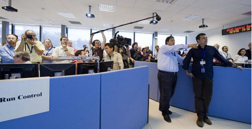
In the movie Groundhog Day, a reporter is forced to re-live a day (February 2) over and over again. Perhaps the coming LHC re-startup would feel like Groundhog Day to some science reporters. CERN therefore has no plans to invite the media here for the first beams this autumn. The first collisions at 450 on 450 GeV (hopefully a short time later) will also be kept low key. What is not fully decided is how to handle the first high-energy collisions and the first events from ATLAS and the other experiments.The images from last September (both control room scenes and the splash events) made a vivid impression on the news media and the public. This time ATLAS will not allow reporters within the Control Room, but the new Visitor Center allows a view of the activities, and new high-quality cameras (mounted on the back wall) can provide the video footage the media wants. The ATLAS website had more than two million hits during the September 2008 activities.Rumors are swirling that Tom Hanks may return to CERN to “turn on” the LHC, but of course that depends on the schedules of Hanks and the LHC. There are several stages in the startup process that could be defined as “turn-on”.Four members of the ATLAS outreach group have been travelling to Sony Pictures (near Hollywood) to help develop a 15-minute CERN/ATLAS “extra” that will be added to the DVD of Angels & Demons that will be released in November. We have also requested to get a copy of the five-minute segment near the beginning of the movie that has some spectacular cinematography of ATLAS. Have you seen our ATLAS webpages on antimatter at http://atlas.ch/angels-demons/ and the new exhibition in the Globe? Finally there have been at least 60 very successful lectures worldwide discussing the science of the movie and the science of LHC.In other news, design work is in progress to replace the aging posters in the Bldg. 40 café. The idea is to make the café an appealing place for physicists to chat and sip coffee, as well as to make it an interesting place to bring visitors to show them the basics of ATLAS.If you haven’t seen modern pop-up books, you will be surprised by the complexity they can portray. ATLAS will soon have its own dramatic pop-up book, a production led by Emma Sanders. It portrays both the detector and the physics.Work is in progress on an animation in the style of the ATLAS animations Episodes I and II. This new project is a joint effort with CMS to portray the physics of the LHC. Two professional animators are working on the project, and a senior person at Pixar has been consulting periodically. Completion date is approximately October 2009. Thought is also being given to an update of the 12-year-old ATLAS movie. All of our videos are on YouTube. Both CERN and ATLAS are working on new/updated communication plans. In the case of CERN, a draft plan has been circulated amongst the experiments. The ATLAS plan is in progress and should be completed in June.These are just the highlights of our activities. You can catch up on the whole series of outreach efforts at the next ATLAS overview week.
Michael Barnett
ATLAS Outreach

sabato 6 giugno 2009

'Colossal' Magnetic Effect Under Pressure


The structure models for F-type and A-type magnetic ordering in manganite in response to pressure. The arrows inside orbitals indicate the spin direction of d electrons.
(PhysOrg.com) -- Millions of people today carry around pocket-sized music players capable of holding thousands of songs, thanks to the discovery 20 years ago of a phenomenon known as the “giant magnetoresistance effect,” which made it possible to pack more data onto smaller and smaller hard drives. Now scientists are on the trail of another phenomenon, called the “colossal magnetoresistance effect” (CMR) which is up to a thousand times more powerful and could trigger another revolution in computing technology.
Understanding, and ultimately controlling, this effect and the intricate coupling between and magnetism in these materials remains a challenge, however, because of competing interactions in manganites, the materials in which CMR was discovered. In the June 12, 2009, issue of the journal Physical Review Letters, a team of researchers report new progress in using high pressure techniques to unravel the subtleties of this coupling.
To study the magnetic properties of manganites, a form of manganese oxide, the research team, led by Yang Ding of the Carnegie Institution’s High Pressure Synergetic Center (HPSync), applied techniques called x-ray magnetic circular dichroism (XMCD) and angular-dispersive diffraction at the (APS) of Argonne National Laboratory in Illinois. High pressure XMCD is a newly developed technique that uses high-brilliance circularly polarized x-rays to probe the magnetic state of a material under pressures of many hundreds of thousands of atmospheres inside a diamond anvil cell.
The discovery of CMR in manganite compounds has already made manganites invaluable components in technological applications. An example is magnetic tunneling junctions in soon-to-be marketed magnetic random access memory (MRAM), where the tunneling of electrical current between two thin layers of manganite material separated by an electrical insulator depends on the relative orientation of magnetization in the manganite layers. Unlike conventional RAM, MRAM could yield instant-on computers. However, no current theories can fully explain the rich physics, including CMR effects, seen in manganites.
“The challenge is that there are competing interactions in manganites among the electrons that determine magnetic properties,” said Ding. “And the properties are also affected by external stimuli, such as, temperature, pressure, magnetic field, and chemical doping.”
“Pressure has a unique ability to tune the electron interactions in a clean and theoretically transparent manner,” he added. “It is a direct and effective means for manipulating the behavior of electrons and could provide valuable information on the magnetic and electronic properties of manganite systems. But of all the effects, pressure effects have been the least explored.”
The researchers found that when a manganite was subjected to conditions above 230,000 times atmospheric pressure it underwent a transition in which its magnetic ordering changed from a ferromagnetic type (electron spins aligned) to an antiferromagnetic type (electron spins opposed). This transition was accompanied by a non-uniform structural distortion called the Jahn-Teller effect.
“It is quite interesting to observe that uniform compression leads to a non-uniform structural change in a manganite, which was not predicted by theory,” said Ding, “Working with Michel van Veenendaal’s theoretical group at APS, we found that the predominant effect of pressure on this material is to increase the strength of an interaction known as superexchange relative to another known as the double exchange interaction. A consequence of this is that the overall ferromagnetic interactions in the system occur in a plane (two dimensions) rather than in three dimensions, which produces a non-uniform redistribution of electrons. This leads to the structural distortion.”
Another intriguing response of manganite to high pressure revealed by the experiments is that the magnetic transition did not occur throughout the sample at the same time. Instead, it spread incrementally.
“The results imply that even at ambient conditions, the manganite might already have two separate magnetic phases at the nanometer scale, with pressure favoring the growth of the antiferro-magnetic phase at the expense of the ferromagnetic phase,” said coauthor Daniel Haskel, a physicist at Argonne’s APS. “Manipulating phase separation at the nanoscale level is at the very core of nanotechnology and manganites provide an excellent playground to pursue this objective”.
“This work not only displays another interesting emergent phenomenon arising from the interplay between charge, spin, orbital and lattice in a strongly correlated electron system,” commented coauthor Dr. Ho-kwang Mao of Carnegie’s Geophysical Laboratory, Director of HPSync,” but it also manifests the role of pressure in magnetism studies of dense matter.”
More information: Pressure-induced magnetic transition in manganite (La0.75Ca0.25MnO3) Yang Ding, Daniel Haskel, Yuan-Chieh Tseng, Eiji Kaneshita, Michel van Veenendaal, John Mitchell, Stanislav V. Sinogeikin, Vitali Prakapenka, and Ho-kwang Mao, Physical Review Letters, June 2009.
Provided by Carnegie Institution

venerdì 5 giugno 2009

Lasers Are Making Solar Cells Competitive

SOURCE

ScienceDaily (June 4, 2009) — Solar electricity has a bright future: It is renewable and available in unlimited quantities, and it does not produce any gases detrimental to the climate. Its only drawback right now is the price: the electric power currently being produced by solar cells in northern Europe must be subsidized if it is to compete against the household electricity generated by traditional power plants. At "Laser 2009" in Munich, June 15 to 18, Fraunhofer researchers will be demonstrating how laser technology can contribute to optimizing the manufacturing costs and efficiency of solar cells.
Cell phones, computers, MP3 players, kitchen stoves, and irons all have one thing in common: They need electricity. And in the future, more and more cars will also be fuelled by electric power. If the latest forecast from the World Energy Council WEC can be believed, global electricity requirements will double in the next 40 years. At the same time, prices for the dwindling resources of petroleum and natural gas are climbing.
“Rising energy prices are making alternative energy sources increasingly cost-effective. Sometime in the coming years, renewable energy sources, such as solar energy, will be competitive, even without subsidization,” explains Dr. Arnold Gillner, head of the microtechnology department at the Fraunhofer Institute for Laser Technology in Aachen, Germany. “Experts predict that grid parity will be achieved in a few years. This means that the costs and opportunities in the grid will be equal for solar electricity and conventionally generated household electricity.” Together with his team at the Fraunhofer Institute for Laser Technology ILT in Aachen, this researcher is developing technologies now that will allow faster, better, and cheaper production of solar cells in the future. “Lasers work quickly, precisely, and without contact. In other words, they are an ideal tool for manufacturing fragile solar cells. In fact, lasers are already being used in production today, but there is still considerable room for process optimization.” In addition to gradually improving the manufacturing technology, the physicists and engineers in Aachen are working with solar cell developers - for example, at the Fraunhofer Institute for Solar Energy Systems ISE in Freiburg - on new engineering and design alternatives.
New production technologies allow new design alternatives
At “Laser 2009” in Munich, the researchers will be demonstrating how lasers can drill holes into silicon cells at breathtaking speed: The ILT laser system drills more than 3,000 holes within one second. Because it is not possible to move the laser source at this speed, the experts have developed optimized manufacturing systems which guide and focuses the light beam at the required points. “We are currently experimenting with various laser sources and optical systems,” Gillner explains. “Our goal is to increase the performance to 10,000 holes a second. This is the speed that must be reached in order to drill 10,000 to 20,000 holes into a wafer within the cycle time of the production machines.”
The tiny holes in the wafer - their diameter is only 50 micrometers – open up undreamt-of possibilities for the solar cell developers. “Previously, the electrical contacts were arranged on the top of the cells. The holes make it possible to move the contacts to the back, with the advantage that the electrodes, which currently act as a dark grid to absorb light, disappear. And so the energy yield increases. The goal is a degree of efficiency of 20 percent% in industrially-produced emitter wrap-through (EWT) cells, with a yield of one-third more than classic silicon cells,” Gillner explains. The design principle itself remains unchanged: In the semi-conductor layer, light particles, or photons, produce negative electrons and positive holes, each of which then wanders to the oppositely poled electrodes. The contacts for anodes and cathodes in the EWT cells are all on the back, there is no shading caused by the electrodes, and the degree of efficiency increases. With this technique, it may one day be possible to use unpurified “dirty” silicon to manufacture solar cells that have poorer electrical properties, but that are cheaper.
Drilling holes into silicon cells is only one of many laser applications in solar cell manufacturing. In the EU project Solasys – Next Generation Solar Cell and Module Laser Processing Systems – an international research team is currently developing new technologies that will allow production to be optimized in the future. ILT in Aachen is coordinating the six million euro project. “We are working on new methods that make the doping of semiconductors, the drilling and the surface structuring of silicon, the edge isolation of the cells, and the soldering of the modules more economical,” project coordinator Gillner explains. For example, “selective laser soldering” makes it possible to improve the rejection rates and quality of the contacting, and so reduce manufacturing costs. Until now, the electrodes were mechanically pressed onto the cells, and then heated in an oven. “But silicon cells often break during this process,” Gillner knows. “Breakage is a primary cost factor in production.” On the other hand, however, with “selective laser soldering” the contacts are pressed on to the cells with compressed air and then soldered with the laser. The mechanical stress approaches zero and the temperature can be precisely regulated. The result: Optimal contacts and almost no rejects.
Laser technology means more efficient thin film cells
Laser technology is also helping to optimize the manufacture of thin film solar cells. The extremely thin film packages made of semiconducting oxide, amorphous silicon, and metal that are deposited onto the glass panels still have a market share of only ten percent. But as Gillner knows, “This could be higher, because thin film solar cells can be used anywhere that non-transparent glass panels can be mounted, for example, on house facades or sound-insulating walls. But the degrees of efficiency are comparable low at five to eight percent, and the production costs are comparatively high.” The laser researchers are working to improve these costs. Until now, the manufacturers have used mechanical methods or solid-state lasers in the nanosecond range in order to structure the active layers on the glass panels. In order to produce electric connections between the semiconductor and the metal, grooves only a few micrometers wide must be created. At the Fraunhofer-Gesellschaft booth at “Laser 2009” the ILT researchers will be demonstrating a 400-watt ultrashort pulse laser that processes thin-film solar modules ten times faster than conventional diode-pumped solid-state lasers. “The ultrashort pulse laser is an ideal tool for ablating thin layers: It works very precisely, does not heat the material and, working with a pulse frequency of 80 MHz, can process a 2-by-3 meter glass panel in under two minutes,” Gillner reports. “The technology is still very new, and high-performance scanning systems and optical systems adapted to the process must be developed first. In the medium term, however, this technology will be able to reduce production costs.”
The rise of laser technology in solar technology is just taking off, and it still has a long way to go. “Lasers simplify and optimize the manufacture of classic silicon and thin-film cells, and they allow the development of new design alternatives,” Gillner continues. “And so laser technology is making an important contribution towards allowing renewable energy sources to penetrate further into the energy market.”
Adapted from materials provided by Fraunhofer-Gesellschaft.

venerdì 29 maggio 2009

Regular Light Bulbs Made Super-Efficient with Ultra-Fast Laser

SOURCE

Chunlei Guo stands in front of his femtosecond laser, which can double the efficiency of a regular incandescent light bulb. Credit: University of Rochester
(PhysOrg.com) -- An ultra-powerful laser can turn regular incandescent light bulbs into power-sippers, say optics researchers at the University of Rochester. The process could make a light as bright as a 100-watt bulb consume less electricity than a 60-watt bulb while remaining far cheaper and radiating a more pleasant light than a fluorescent bulb can.
The laser process creates a unique array of nano- and micro-scale structures on the surface of a regular tungsten filament—the tiny wire inside a light bulb—and theses structures make the tungsten become far more effective at radiating light.
The findings will be published in an upcoming issue of the journal .
"We've been experimenting with the way ultra-fast lasers change metals, and we wondered what would happen if we trained the laser on a filament," says Chunlei Guo, associate professor of optics at the University of Rochester. "We fired the right through the glass of the bulb and altered a small area on the filament. When we lit the bulb, we could actually see this one patch was clearly brighter than the rest of the filament, but there was no change in the bulb's energy usage."
The key to creating the super-filament is an ultra-brief, ultra-intense beam of light called a femtosecond laser pulse. The laser burst lasts only a few quadrillionths of a second. To get a grasp of that kind of speed, consider that a femtosecond is to a second what a second is to about 32 million years. During its brief burst, Guo's laser unleashes as much power as the entire grid of North America onto a spot the size of a needle point. That intense blast forces the surface of the metal to form nanostructures and microstructures that dramatically alter how efficiently can radiate from the filament.
In 2006, Guo and his assistant, Anatoliy Vorobeyv, used a similar laser process to turn any metal pitch black. The surface structures created on the metal were incredibly effective at capturing incoming radiation, such as light.
"There is a very interesting 'take more, give more' law in nature governing the amount of light going in and coming out of a material," says Guo. Since the black metal was extremely good at absorbing light, he and Vorobyev set out to study the reverse process—that the blackened filament would radiate light more effectively as well.
"We knew it should work in theory," says Guo, "but we were still surprised when we turned up the power on this bulb and saw just how much brighter the processed spot was."
In addition to increasing the brightness of a bulb, Guo's process can be used to tune the color of the light as well. In 2008, his team used a similar process to change the color of nearly any metal to blue, golden, and gray, in addition to the black he'd already accomplished. Guo and Vorobeyv used that knowledge of how to control the size and shape of the nanostructures—and thus what colors of light those structures absorb and radiate—to change the amount of each wavelength of light the tungsten filament radiates. Though Guo cannot yet make a simple bulb shine pure blue, for instance, he can change the overall radiated spectrum so that the tungsten, which normally radiates a yellowish light, could radiate a more purely white light.
Guo's team has even been able to make a filament radiate partially polarized light, which until now has been impossible to do without special filters that reduce the bulb's efficiency. By creating nanostructures in tight, parallel rows, some light that emits from the filament becomes polarized.
The team is now working to discover what other aspects of a common light bulb they might be able to control. Fortunately, despite the incredible intensity involved, the femtosecond laser can be powered by a simple wall outlet, meaning that when the process is refined, implementing it to augment regular light bulbs should be relatively simple.
Guo is also announcing this month in Applied Physics Letters a technique using a similar femtosecond process to make a piece of metal automatically move liquid around its surface, even lifting a liquid up against gravity.
Source: University of Rochester (news : web)

World's largest laser opens: We are close to practice the nuclear fusion


Scientists for decades have been hunting for ways to harness the enormous force of the sun and stars to supply energy here on Earth. The National Ignition Facility at the Lawrence Livermore Laboratory may spark the light at the end of the tunnel.
The facility was dedicated today (May 29) at a ceremony attended by numerous state and national officials.
Roughly the size of three football fields, the facility houses the world’s largest laser. Within the next three years, its 192 laser beams will deliver massive amounts of at a pea-sized target. That target, filled with , will in turn release 10 to 100 times the power than the amount injected by the laser.

When all of the lasers’ energy slams the target, it will generate unprecedented temperatures in the target materials - temperatures of more than 100 million degrees and pressures more than 100 billion times the Earth’s atmosphere. These conditions are similar to those in the stars and the cores of . Igniting these conditions will create nuclear fusion, which is the reaction that gives the sun and the stars their immense power. Mimicking and controlling the highly volatile process - tantamount to creating a star in a laboratory - could lead to ways to produce plentiful clean and safe energy.
While demonstrating nuclear fusion as a viable means for abundant clean energy may be the most exciting offshoot of NIF research, another of its roles is to study the conditions associated with the inner workings of nuclear weapons.
The NIF is a cornerstone of a critical national security mission to ensure the reliability and safety of the U.S. nuclear stockpile without conducting underground testing. At NIF, scientists will be able to provide data for supercomputer simulations that replicate conditions that exist inside a thermonuclear weapon.
NIF experiments will also help scientists who are trying to understand the universe in many fundamental ways, including astrophysicists learning about the hot, dense interiors of large planets, stars and other phenomena.
Provided by University of California

lunedì 11 maggio 2009

Ultra-dense Deuterium May Be Nuclear Fuel Of The Future

SOURCE

ScienceDaily (May 12, 2009) — A material that is a hundred thousand times heavier than water and more dense than the core of the Sun is being produced at the University of Gothenburg. The scientists working with this material are aiming for an energy process that is both more sustainable and less damaging to the environment than the nuclear power used today.
Imagine a material so heavy that a cube with sides of length 10 cm weights 130 tonnes, a material whose density is significantly greater than the material in the core of the Sun. Such a material is being produced and studied by scientists in Atmospheric Science at the Department of Chemistry, the University of Gothenburg.
Towards commercial use
So far, only microscopic amounts of the new material have been produced. New measurements that have been published in two scientific journals, however, have shown that the distance between atoms in the material is much smaller than in normal matter. Leif Holmlid, Professor in the Department of Chemistry, believes that this is an important step on the road to commercial use of the material.
The material is produced from heavy hydrogen, also known as deuterium, and is therefore known as “ultra-dense deuterium”. It is believed that ultra-dense deuterium plays a role in the formation of stars, and that it is probably present in giant planets such as Jupiter.
An efficient fuel
So what can this super-heavy material be used for?
“One important justification for our research is that ultra-dense deuterium may be a very efficient fuel in laser driven nuclear fusion. It is possible to achieve nuclear fusion between deuterium nuclei using high-power lasers, releasing vast amounts of energy”, says Leif Holmlid.
The laser technology has long been tested on frozen deuterium, known as “deuterium ice”, but results have been poor. It has proved to be very difficult to compress the deuterium ice sufficiently for it to attain the high temperature required to ignite the fusion.
Energy source of the future
Ultra-dense deuterium is a million times more dense than frozen deuterium, making it relatively easy to create a nuclear fusion reaction using high-power pulses of laser light.
“If we can produce large quantities of ultra-dense deuterium, the fusion process may become the energy source of the future. And it may become available much earlier than we have thought possible”, says Leif Holmlid.
“Further, we believe that we can design the deuterium fusion such that it produces only helium and hydrogen as its products, both of which are completely non-hazardous. It will not be necessary to deal with the highly radioactive tritium that is planned for use in other types of future fusion reactors, and this means that laser-driven nuclear fusion as we envisage it will be both more sustainable and less damaging to the environment than other methods that are being developed.”
Deuterium – brief facts
Deuterium is an isotope of hydrogen that is found in large quantities in water, more than one atom per ten thousand hydrogen atoms has a deuterium nucleus. The isotope is denoted “2H” or “D”, and is normally known as “heavy hydrogen”. Deuterium is used in a number of conventional nuclear reactors in the form of heavy water (D2O), and it will probably also be used as fuel in fusion reactors in the future.
Adapted from materials provided by University of Gothenburg.

domenica 10 maggio 2009

The Laser Glow of an Atom Cloud

SOURCE


Random lasers are the "disco ball" version of normal lasers. Instead of beaming in one direction, the light is scattered out in all directions by particles in a powder, for example. Calculations described in the 1 May Physical Review Letters show that a cloud of cold atoms could form a new type of random laser, where individual atoms scatter and amplify the light. The work suggests that the atoms will begin lasing if the cloud can be made opaque, or "cloudy," enough, which the authors think is within reach of current technology. Because such a system is fundamentally simple, it may give insight into some of the mysteries of random lasers.
A normal laser is essentially a gain medium inside a reflective cavity. The light is amplified by the medium as it bounces back and forth between the cavity's mirrors. A random laser has no cavity. Instead, tiny "mirrors," or scatterers, are added to the gain medium, causing photons to bounce around and become amplified by the medium, before escaping in all directions. For example, a container of micron-sized particles floating in water in which a laser dye has also been dissolved can emit laser light if pumped with external light. Random lasers do not require the same precise manufacturing as normal lasers, so they could be inexpensive to produce. Potential applications include digital displays, light emitting paints, and temperature sensors.
There are, however, some uncertainties regarding the spectra and time variability of random lasers [see Focus story: "Photon Marathon"]. So Robin Kaiser of Nice Sophia Antipolis University and the National Center for Scientific Research (CNRS) in France and his colleagues considered a random laser made up of cold atoms. Such a system would not have the absorption and other difficult-to-model complexities of existing random lasers. However, "it was not clear that atoms would be able to play the roles of both gain medium and scatterers," says Nice team member William Guerin. A single atom scatters photons when it's in its ground state and amplifies photons (through stimulated emission) when it's in an excited state, but it can't do both at the same time. So the researchers needed to find the right balance of atoms in both ground and excited states.
The team modeled a two-level atomic system. In their scenario, a complicated three-photon transition--made possible by an external pump laser--keeps a sufficient fraction of the atoms in the excited state (a so-called population inversion) from which they can provide gain. For different pump frequencies and intensities, the researchers calculated the amount of scattering necessary to trap light in the cloud long enough for it to become true "coherent" laser light, with all the photons propagating in synch. They quantified the amount of scattering within the cloud with a number called the optical thickness [1]. A value between 200 and 250 would lead to lasing, they found, which is within reach of state-of-the-art cold atom traps that currently achieve 150, Guerin says.
The researchers performed a simulation showing that the laser light should be detectable over background light coming from the cloud. They are now trying to make such a random laser in the lab using a standard magneto-optical trap to hold the atoms. Guerin says there are tricks to compress the trap to increase the density and therefore the amount of scattering.
There may, however, be experimental challenges involving the non-uniform density of the cloud, says Diederik Wiersma of the European Laboratory for Non-linear Spectroscopy in Florence, Italy. But if it can work, the use of atoms, rather than micron-scale scatterers, "could enrich our understanding of the random laser phenomena," Wiersma says. Moreover, because cold atoms are capable of slowing down light, he speculates that they could be more efficient at trapping light than current techniques. --Michael Schirber Michael Schirber is a freelance science writer in Lyon, France.
References:[1] The optical thickness--a characterization of the "opaqueness" of the atoms--can be thought of as the diameter of the cloud measured in units of the "mean free path," which is the typical distance a photon travels before scattering. This refers to scattering with the pump laser turned off, when there is no lasing.
Related Information:Related info:
Focus story: Photon Marathon (2004)
more explanation of random lasers from Wiersma's lab web site
Threshold of a Random Laser with Cold Atoms Luis S. Froufe-Pérez, William Guerin, Rémi Carminati, and Robin Kaiser Phys. Rev. Lett. 102, 173903 (issue of 1 May 2009)

A Light Touch

SOURCE


Magnetically encoded information is at the core of much modern technology, and researchers are always looking for better ways to manipulate it. In the 8 May Physical Review Letters, a German team shows that a surprisingly feeble light beam can flip zeros to ones and vice versa, in a special magnetic layer. Although currently limited to very low temperatures, the apparently new effect might one day be extended to improve data storage.
Most familiar magnets are metals. They contain atoms that host tiny magnetic bar magnets, or moments, that can point up or down, and the atoms are surrounded by a sea of electrons. But researchers have long been interested in a different type of magnet, one consisting of widely separated magnetic ions embedded in a semiconductor. Unlike a metal, the number of free electrons in a semiconductor changes when it's exposed to electric current or light, so these materials should provide new ways to influence the magnetic properties, via the electrons. Light can flip the magnetization--the total magnetic moment of atoms in a region--from up to down, for example. But until now, experimenters needed very bright light to weaken the magnetization enough to reorient it.
In the new research, a team led by Laurens Molenkamp of the University of Würzburg in Germany grew a thin, crystalline layer of the common semiconductor gallium arsenide but replaced about one percent of the gallium atoms with the magnetic atom manganese. At temperatures below about 25 Kelvin, this layer acts as a ferromagnet: the magnetic moments on different manganese atoms point in the same direction, either up from the surface or down into it. The magnetization direction persists even when the researchers apply an opposing magnetic field, as long as the field does not exceed a threshold called the coercive field.
But when the team focused the light from a standard red laser on the film, the magnetization in the illuminated spot changed direction to match the magnetic field-- opposite to the rest of the film. The light didn’t change the strength of the magnetization, the team found, but instead reduced the field strength needed to flip it.
A mundane explanation would be that the light simply heats the film, which decreases the coercive field. To check this possibility, the team monitored the size of the magnetically flipped spot over many seconds of illumination. "It grows rather slowly," notes Würzburg team member Georgy Astakhov. "Heat diffusion occurs much, much faster." Instead, the team proposes that electrons liberated by the light (and the "holes" they leave behind) affect the magnetization directly. These charge carriers, they suggest, are quickly trapped in regions with high or low manganese concentration. These trapped charges effectively grease the motion of the "domain wall" that separates regions of opposite magnetization, by smoothing out local variations that would otherwise impede its motion. When the domain wall can move smoothly, a region with magnetization pointing up can more easily spread at the expense of a neighboring region having oppositely-directed magnetization.
Theo Rasing, of Radboud University in Nijmegen, Netherlands, says that more work is needed to confirm this non-thermal explanation, including extending the experiment to more than one sample. He also notes that because the dim light is on for a long time, the energy needed to flip the magnetization is not so different from other experiments that use very bright but short light pulses. Nonetheless, Rasing says that seeing a non-thermal change in magnetism with such a dim beam expands such "opto-magnetic" effects to new materials and mechanisms and should inspire further experiments by others.--Don Monroe Don Monroe is a freelance science writer in Murray Hill, New Jersey.
Related Information:
Physics Viewpoint essay by Molenkamp: Convincing a Magnetic Semiconductor to Work at Room Temperature (December, 2008)
Focus story on another optical magnetization flipping technique: Flipping Atoms Fast (1999)
Nonthermal Photocoercivity Effect in a Low-Doped (Ga,Mn)As Ferromagnetic Semiconductor G. V. Astakhov, H. Hoffmann, V. L. Korenev, T. Kiessling, J. Schwittek, G. M. Schott, C. Gould, W. Ossau, K. Brunne, and L. W. Molenkamp Phys. Rev. Lett. 102, 187401 (issue of 8 May 2009)

sabato 9 maggio 2009

Carbon Nanotubes: Innovative Technology Or Risk To Health Or Environment?


ScienceDaily (May 10, 2009) — Carbon nanotubes have made a meteoric career in the past 15 years, even if their applications are still limited. Recent research results show that – apart from their favorable mechanical and electrical properties – they also have disadvantageous characteristics.
One aspect which has rarely been considered so far is now addressed by researchers of the research center Forschungszentrum Dresden-Rossendorf. “If the application of products and commodities containing carbon nanotubes will increase in the future, then there will be a higher probability for the tubes to get into the environment during their production, usage or disposal, to be distributed there, and to bind pollutants such as heavy metals on their way trough the environment”, says Harald Zaenker, scientist at the FZD.
Via water into the environment
An important way for carbon nanotubes of getting into the environment is the way via the water. In their original state, the flimsy carbon fibers with a diameter of less than 50 nanometers (1 nanometer = 1 millionth of a millimeter) are hardly water-soluble. At first glance, they should therefore not be mobile in groundwater, lakes etc., i.e. they should rapidly settle or deposit. However, carbon nanotubes are able to form colloidal solutions if their surface structure is changed. Changes in the surface structure can be brought about deliberately during the production of the tubes or can be induced by natural processes if the tubes are released into the environment.
A colloidal solution, unlike a true solution of water-soluble substances, is a solution in which the apparently dissolved substance is finely dispersed in the solvent forming tiny particles. These particles are still much bigger than the molecules of a dissolved substance in a true solution. As colloids, carbon nanotubes might be transported anywhere in environmental waters. It is known meanwhile that the tubes can even penetrate cell walls and, thus, might theoretically be able to enter also animal or human cells. In addition, changes in the surface structure of carbon nanotubes cause another effect: their capability to bind heavy metals is increased.
Tubes with changed surface
The scientists investigated carbon nanotubes both in their original state and in a state changed by oxidizing acids (such as a mixture of nitric and sulfuric acid). They found out that solutions of treated carbon nanotubes scatter light more strongly. “This is an indication that colloids have formed which do not settle”, Harald Zaenker says.
The researchers provided evidence for the first time that the heavy metal uranium, which is ubiquitous in the environment and, hence, also in the water, is particularly attached to the surface of treated carbon nanotubes. The scientists found out that the uranium uptake capacity is increased by an order of magnitude in comparison to untreated carbon nanotubes. “Therefore, it is plausible to assume that carbon nanotubes, if released to the environment, influence the transport of uranium in environmental waters and even in biological systems. The possible impact on the environment and on human health has in general been considered too little”, Harald Zaenker says.
On the other hand, the high bonding capacity of carbon nanotubes for uranium and other heavy metals also suggests using them for the removal of heavy metals from waters. However, they are not yet a cost-efficient alternative to classic water purifiers, Zaenker says. “Eventually, it is important to further study the behavior of carbon nanotubes in waters”, the scientist says. “Only then can the positive and negative aspects of carbon nanotubes be better assessed.”
Journal reference:
Schierz et al. Aqueous suspensions of carbon nanotubes: Surface oxidation, colloidal stability and uranium sorption. Environmental Pollution, 2009; 157 (4): 1088 DOI: 10.1016/j.envpol.2008.09.045
Adapted from materials provided by Forschungszentrum Dresden Rossendorf.

mercoledì 31 ottobre 2007

Star Trek Gadget? 'Tractor Beam' For Cells Developed


Source:

ScienceDaily (Oct. 31, 2007) — In a feat that seems like something out of a microscopic version of Star Trek, MIT researchers have found a way to use a “tractor beam” of light to pick up, hold, and move around individual cells and other objects on the surface of a microchip.
The new technology could become an important tool for both biological research and materials research, say Matthew J. Lang and David C. Appleyard, whose work is being published in the journal Lab on a Chip.
The idea of using light beams as tweezers to manipulate cells and tiny objects has been around for at least 30 years. But the MIT researchers have found a way to combine this powerful tool for moving, controlling and measuring objects with the highly versatile world of microchip design and manufacturing.
Optical tweezers, as the technology is known, represent “one of the world's smallest microtools,” says Lang. “Now, we're applying it to building [things] on a chip.”
Says Appleyard, “We've shown that you could merge everything people are doing with optical trapping with all the exciting things you can do on a silicon wafer…There could be lots of uses at the biology-and-electronics interface.”
For example, he said, many people are studying how neurons communicate by depositing them on microchips where electrical circuits etched into the chips monitor their electrical behavior. “They randomly put cells down on a surface, and hope one lands on [or near] a [sensor] so its activity can be measured. With [our technology], you can put the cell right down next to the sensors.” Not only can motions be precisely controlled with the device, but it can also provide very precise measurements of a cell's position.
Optical tweezers use the tiny force of a beam of light from a laser to push around and control tiny objects, from cells to plastic beads. They usually work on a glass surface mounted inside a microscope so that the effects can be observed.
But silicon chips are opaque to light, so applying this technique to them not an obvious move, the researchers say, since the optical tweezers use light beams that have to travel through the material to reach the working surface. The key to making it work in a chip is that silicon is transparent to infrared wavelengths of light - which can be easily produced by lasers, and used instead of the visible light beams.
To develop the system, Lang and Appleyard weren't sure what thickness and surface texture of wafers, the thin silicon slices used to manufacture microchips, would work best, and the devices are expensive and usually available only in quantity. “Being at MIT, where there is such a strength in microfabrication, I was able to get wafers that had been thrown out,” Appleyard says. “I posted signs saying, 'I'm looking for your broken wafers'.”
After testing different samples to determine which worked best, they were able to order a set that were just right for the work. They then tested the system with a variety of cells and tiny beads, including some that were large by the standards of optical tweezer work. They were able to manipulate a square with a hollow center that was 20 micrometers, or millionths of a meter, across - allowing them to demonstrate that even larger objects could be moved and rotated. Other test objects had dimensions of only a few nanometers, or billionths of a meter. Virtually all living cells come in sizes that fall within that nanometer-to-micrometers range and are thus subject to being manipulated by the system.
As a demonstration of the system's versatility, Appleyard says, they set it up to collect and hold 16 tiny living E. coli cells at once on a microchip, forming them into the letters MIT.
Lang is an assistant professor in the Department of Biological Engineering and the Department of Mechanical Engineering. Appleyard is a graduate student in Biological Engineering.
The work was supported by the Biotechnology Training Program of the National Institutes of Health, the W.M. Keck Foundation, and MIT's Lincoln Laboratory.
Adapted from materials provided by Massachusetts Institute Of Technology.

Fausto Intilla
www.oloscience.com

giovedì 25 ottobre 2007

Quantum Cascade Laser Nanoantenna Created


Source:

ScienceDaily (Oct. 25, 2007) — In a major feat of nanotechnology engineering researchers from Harvard University have demonstrated a laser with a wide-range of potential applications in chemistry, biology and medicine. Called a quantum cascade (QC) laser nanoantenna, the device is capable of resolving the chemical composition of samples, such as the interior of a cell, with unprecedented detail.
Spearheaded by graduate students Nanfang Yu, Ertugrul Cubukcu, and Federico Capasso, Robert L. Wallace Professor of Applied Physics, all of Harvard's School of Engineering and Applied Sciences, the findings will be published as a cover feature of the October 22 issue of Applied Physics Letters. The researchers have also filed for U.S. patents covering this new class of photonic devices.
The laser's design consists of two gold rods separated by a nanometer gap (a device known as an optical antenna) built on the facet of a quantum cascade laser, which emits invisible light in the region of the spectrum where most molecules have their tell tale absorption fingerprints. The nanoantenna creates a light spot of nanometric size about fifty to hundred times smaller than the laser wavelength; the spot can be scanned across a specimen to provide chemical images of the surface with superior spatial resolution.
"There's currently a major push to develop powerful tabletop microscopes with spatial resolution much smaller than the wavelength that can provide images of materials, and in particular biological specimens, with chemical information on a nanometric scale," says Federico Capasso.
While infrared microscopes, based on the detection of molecular absorption fingerprints, are commercially available and widely used to map the chemical composition of materials, their spatial resolution is limited by the range of available light sources and optics to well above the wavelength. Likewise the so-called near field infrared microscopes, which rely on an ultra sharp metallic tip scanned across the sample surface at nanometric distances, can provide ultrahigh spatial resolution but applications are so far strongly limited by the use of bulky lasers with very limited tunability and wavelength coverage.
"By combining Quantum Cascade Lasers with optical antenna nanotechnology we have created for the first time an extremely compact device that will enable the realization of new ultrahigh spatial resolution microscopes for chemical imaging on a nanometric scale of a wide range of materials and biological specimens," says Capasso.
Quantum cascade (QC) lasers were invented and first demonstrated by Capasso and his group at Bell Labs in 1994. These compact millimeter length semiconductor lasers, which are now commercially available, are made by stacking nanometer thick layers of semiconductor materials on top of each other. By varying the thickness of the layers one can select the wavelength of the QC laser across essentially the entire infrared spectrum where molecules absorb, thus custom designing it for a specific application.
In addition by suitable design the wavelength of a particular QCL can be made widely tunable. The range of applications of QC laser based chemical sensors is very broad, including pollution monitoring, chemical sensing, medical diagnostics such as breath analysis, and homeland security.
The teams co-authors are Kenneth Crozier, Assistant Professor of Electrical Engineering, and research associates Mikhail Belkin and Laurent Diehl, all of Harvard's School of Engineering and Applied Sciences; David Bour, Scott Corzine, and Gloria Höfler, all formerly with Agilent Technologies. The research was supported by the Air Force Office of Scientific Research and the National Science Foundation. The authors also acknowledge the support of two Harvard-based centers, the Nanoscale Science and Engineering Center and the Center for Nanoscale Systems, a member of the National Nanotechnology Infrastructure Network.
Adapted from materials provided by Harvard University.

Fausto Intilla

martedì 23 ottobre 2007

Nanowire Generates Its Own Electricity

Source:
ScienceDaily (Oct. 23, 2007) — Harvard chemists have built a new wire out of photosensitive materials that is hundreds of times smaller than a human hair. The wire not only carries electricity to be used in vanishingly small circuits, but generates power as well.
Charles M. Lieber, the Mark Hyman Jr. Professor of Chemistry, and colleagues created the nanowire out of three different kinds of silicon with different electrical properties. The silicon is wrapped in layers to create the wire. When light falls on the outer material, a process begins due to the interaction of the core with the shell layers, leading to the creation of electrical charges.
The idea of creating nanoscale photovoltaics is not new, Lieber said, but prior efforts used organic compounds in combination with semiconductor nanostructures that had lower efficiency and that degraded under concentrated sunlight. Lieber’s materials have several advantages, he said. The materials are more efficient, converting 3.4 percent of the sunlight into electricity; they can withstand concentrated light without deteriorating, gaining efficiency up to about 5 percent; and they’re as cheap to make as other related nanoscale photovoltaic devices.
“The real [question] is whether there’s a new geometry that will lead to better photovoltaic technology,” Lieber said. “We worked on coaxial geometry.”
The most recent development builds on Lieber’s considerable prior work on nanoscale devices. He has developed sensors with potential bioterrorism applications that can detect a single virus or other particle, nanowire arrays that can detect signals in individual neurons, and a cracker-sized detector for cancer.
A cheap nanoscale power source broadens the potential applications of such nanoscale devices. Though the tiny photovoltaic cells can generate enough electricity to power a similarly tiny circuit, Lieber said they’re not yet efficient enough to have applications on the scale of commercial power generation.
Commercial solar cells, he said, have efficiencies around 20 percent, compared with 3.4 percent for his nano-solar cells. One avenue of future research, Lieber said, will be to explore ways to boost efficiency of the nanowire photovoltaics. If they can reach 10 to 15 percent, he said, their lower cost of production — they can be made from relatively inexpensive materials and don’t require clean rooms to produce — may make them useful in larger-scale applications.
“There’s no physical reason it couldn’t be higher,” Lieber said. “I’m pretty optimistic that we’ll be able to track down the efficiency issue.”
Until then, Lieber sees a future for the nanowire photovoltaics in niche applications, such as multiple distributed sensors or durable, flexible devices, possibly sewn into clothing or worn as a patch.
“It will have to be unique to be an economically viable application, some place where you want durability and flexibility, where if it gets destroyed, people don’t care,” Lieber said.
The work was described in the Oct. 18 issue of the journal Nature.
Adapted from materials provided by Harvard University.

Fausto Intilla
www.oloscience.com

lunedì 1 ottobre 2007

Breaking The Barrier Toward Nanometer X-ray Resolution


Source:

Science Daily — A team of researchers at the U.S. Department of Energy's Brookhaven National Laboratory have overcome a major obstacle for using refractive lenses to focus x-rays. This method will allow the efficient focusing of x-rays down to extremely small spots and is an important breakthrough in the development of a new, world-leading light source facility that promises advances in nanoscience, energy, biology, and materials research.
At Brookhaven's National Synchrotron Light Source (NSLS), the scientists exceeded a limit on the ability to focus "hard," or high-energy, x-rays known as the "critical angle."
The critical angle is the maximum angle that light can be deflected, or bent, by a single surface. Imagine a beam of laser light traveling toward a glass lens. Depending on the characteristics of the lens material and the angle at which the beam is pointed, the light can be refracted, that is, transmitted through the lens but deflected. However, when this light approaches the lens at angles less than the critical angle, the beam does not pass through the lens but is instead reflected. This results in a maximum deflection angle for light that passes through the lens.
The maximum deflection angle determines the minimum spot size to which x-rays can be focused. This poses a problem for researchers who are using x-rays to study molecules, atoms, and advanced materials at the nanoscale - on the order of billionths of a meter. Such small subjects require tightly focused beams.
"One measure of the quality of an x-ray optic is how small a focused spot it can make," said NSLS researcher Ken Evans-Lutterodt. "The problem is that nature does not allow a single lens to deflect the x-rays very much. This limits how small of a spot you can create, and this translates to some fuzziness in the image. To get a sharper image, you need a lens that's more able to deflect the x-rays."
In 2003, a trio of Brookhaven researchers - Evans-Lutterodt, Aaron Stein, and James Ablett - were the first to notice the critical angle limit while investigating the properties of a so-called kinoform lens for focusing hard x-rays. This efficient type of refractive lens is similar to those found in lighthouses. The research team proposed a solution to the critical angle problem of a compound kinoform lens, and both the problem and proposed solution were also suggested later by other researchers in the field.
In the current publication, the researchers implemented their idea by creating a compound lens from a series of four kinoform lenses placed one after the other. Using this setup at NSLS beamline X13B, they showed that the critical angle can be surpassed with hard x-rays, while still focusing like a single lens.
"Thanks to the excellent fabrication resources at Brookhaven's Center for Functional Nanomaterials and at Alcatel-Lucent, we are able to fabricate the lenses to the precision required," Stein said.
This is an important step for the National Synchrotron Light Source II (NSLS-II), a state-of-the-art synchrotron facility that will produce x-rays up to 10,000 times brighter than those generated by the current NSLS and could lead to advances such as alternative-energy technologies and new drugs for fighting disease. One of the major goals of the facility is to probe materials and molecules with just one-nanometer resolution - a capability needed to study the intricate mechanisms of chemical and biological systems.
"Without exceeding the critical angle, the refractive lens resolution would be limited to 24 nanometers or more," Ablett said. "Even though in this experiment we just barely exceeded this limit, we've shown that it can be done. This is just the first step."
Next, the researchers will measure the resolution their new lens system produces, and will continue to fabricate and test optics that push further beyond the critical angle, and closer to the one-nanometer benchmark.
"We've broken the barrier, now there's still more work to be done to get down to those small x-ray spots," Evans-Lutterodt said. "Hopefully this will be one of the routes that NSLS-II and others will use."
Their results are described online in the September 28, 2007, edition of Physical Review Letters.
Natasha Bozovic, from San Jose State University, also collaborated on this research. Funding was provided by the Office of Basic Energy Sciences within the U.S. Department of Energy's Office of Science.
Note: This story has been adapted from material provided by DOE, Brookhaven National Laboratory.

Fausto Intilla
www.oloscience.com

venerdì 28 settembre 2007

Quantum Device Traps, Detects And Manipulates The Spin Of Single Electrons


Source:

Science Daily — A novel device, developed by a team led by University at Buffalo engineers, simply and conveniently traps, detects and manipulates the single spin of an electron, overcoming some major obstacles that have prevented progress toward spintronics and spin-based quantum computing.
Published online recently in Physical Review Letters, the research paper brings closer to reality electronic devices based on the use of single spins and their promise of low-power/high-performance computing.
"The task of manipulating the spin of single electrons is a hugely daunting technological challenge that has the potential, if overcome, to open up new paradigms of nanoelectronics," said Jonathan P. Bird, Ph.D., professor of electrical engineering in the UB School of Engineering and Applied Sciences and principal investigator on the project. "In this paper, we demonstrate a novel approach that allows us to easily trap, manipulate and detect single-electron spins, in a scheme that has the potential to be scaled up in the future into dense, integrated circuits."
While several groups have recently reported the trapping of a single spin, they all have done so using quantum dots, nanoscale semiconductors that can only demonstrate spin trapping in extremely cold temperatures, below 1 degree Kelvin.
The cooling of devices or computers to that temperature is not routinely achievable, Bird said, and it makes systems far more sensitive to interference.
The UB group, by contrast, has trapped and detected spin at temperatures of about 20 degrees Kelvin, a level that Bird says should allow for the development of a viable technology, based on this approach.
In addition, the system they developed requires relatively few logic gates, the components in semiconductors that control electron flow, making scalability to complex integrated circuits very feasible.
The UB researchers achieved success through their innovative use of quantum point contacts: narrow, nanoscale constrictions that control the flow of electrical charge between two conducting regions of a semiconductor.
"It was recently predicted that it should be possible to use these constrictions to trap single spins," said Bird. "In this paper, we provide evidence that such trapping can, indeed, be achieved with quantum point contacts and that it may also be manipulated electrically."
The system they developed steers the electrical current in a semiconductor by selectively applying voltage to metallic gates that are fabricated on its surface.
These gates have a nanoscale gap between them, Bird explained, and it is in this gap where the quantum point contact forms when voltage is applied to them.
By varying the voltage applied to the gates, the width of this constriction can be squeezed continuously, until it eventually closes completely, he said.
"As we increase the charge on the gates, this begins to close that gap," explained Bird, "allowing fewer and fewer electrons to pass through until eventually they all stop going through. As we squeeze off the channel, just before the gap closes completely, we can detect the trapping of the last electron in the channel and its spin."
The trapping of spin in that instant is detected as a change in the electrical current flowing through the other half of the device, he explained.
"One region of the device is sensitive to what happens in the other region," he said.
Now that the UB researchers have trapped and detected single spin, the next step is to work on trapping and detecting two or more spins that can communicate with each other, a prerequisite for spintronics and quantum computing.
Co-authors on the paper are Youngsoo Yoon, Ph.D., a UB doctoral student in electrical engineering; L. Mourokh of Queens College and the College of Staten Island of the City University of New York; T. Morimoto, N. Aoki and Y. Ochiai of Chiba University in Japan; and J. L. Reno of Sandia National Laboratories.
The research was funded by the U.S. Department of Energy. Bird, who also has received funding from the UB Office of the Vice President for Research, was recruited to UB with a faculty recruitment grant from the New York State Office of Science, Technology and Academic Outreach (NYSTAR).
Note: This story has been adapted from material provided by University at Buffalo.

Fausto Intilla

martedì 18 settembre 2007

Accepted Notion Of Neutron's Electrical Properties Overturned By New Research

Source:

Science Daily — For two generations of physicists, it has been a standard belief that the neutron, an electrically neutral elementary particle and a primary component of an atom, actually carries a positive charge at its center and an offsetting negative charge at its outer edge.
The notion was first put forth in 1947 by Enrico Fermi, a Nobel laureate noted for his role in developing the first nuclear reactor. But new research by a University of Washington physicist shows the neutron's charge is not quite as simple as Fermi believed.
Using precise data recently gathered at three different laboratories and some new theoretical tools, Gerald A. Miller, a UW physics professor, has found that the neutron has a negative charge both in its inner core and its outer edge, with a positive charge sandwiched in between to make the particle electrically neutral.
"Nobody realized this was the case," Miller said. "It is significant because it is a clear fact of nature that we didn't know before. Now we know it."
The discovery changes scientific understanding of how neutrons interact with negatively charged electrons and positively charged protons. Specifically, it has implications for understanding the strong force, one of the four fundamental forces of nature (the others are the weak force, electromagnetism and gravity).
The strong force binds atomic nuclei together, which makes it possible for atoms, the building blocks of all matter, to assemble into molecules.
"We have to understand exactly how the strong force works, because it is the strongest force we know in the universe," Miller said.
The findings are based on data collected at the Thomas Jefferson National Accelerator Facility in Newport News, Va., the Bates Linear Accelerator at the Massachusetts Institute of Technology and the Mainz Microtron at Johannes Gutenberg University in Germany.
The three labs examine various aspects of the properties and behavior of subatomic particles, and Miller studied data they collected about neutrons. His analysis was published online Sept. 13 in Physical Review Letters. The work was funded in part by the U.S. Department of Energy.
Since the analysis is based on data gathered from direct observations, the picture could change even more as more data are collected, Miller said.
"A particle can be electrically neutral and still have properties related to charge. We've known for a long time that the neutron has those properties, but now we understand them more clearly," he said.
He noted that the most important aspect of the finding confirms that a neutron carries a negative charge at its outer edge, a key piece of Fermi's original idea.
The strong force that binds atomic nuclei is related to nuclear energy and nuclear weapons, and so it is possible the research could have practical applications in those areas.
It also could lend to greater understanding of the interactions that take place in our sun's nuclear furnace, and a greater understanding of the strong force in general, Miller said.
"We already know that without the strong force you wouldn't have atoms -- or anything else that follows from atoms," he said.
This research was published online Sept. 13 in Physical Review Letters. The work was funded in part by the U.S. Department of Energy.
Note: This story has been adapted from a news release issued by University of Washington.

Fausto Intilla
www.oloscience.com